Please wait a minute...
Chin. Phys. B, 2020, Vol. 29(10): 107102    DOI: 10.1088/1674-1056/abaee7
CONDENSED MATTER: ELECTRONIC STRUCTURE, ELECTRICAL, MAGNETIC, AND OPTICAL PROPERTIES Prev   Next  

Effect of source temperature on phase and metal–insulator transition temperature of vanadium oxide films grown by atomic layer deposition

Bingheng Meng(孟兵恒), Dengkui Wang(王登魁)†, Deshuang Guo(郭德双), Juncheng Liu(刘俊成), Xuan Fang(方铉), Jilong Tang(唐吉龙), Fengyuan Lin(林逢源), Xinwei Wang(王新伟), Dan Fang(房丹), and Zhipeng Wei(魏志鹏)‡
1 State Key Laboratory of High Power Semiconductor Laser, Changchun University of Science and Technology, Changchun 130022, China
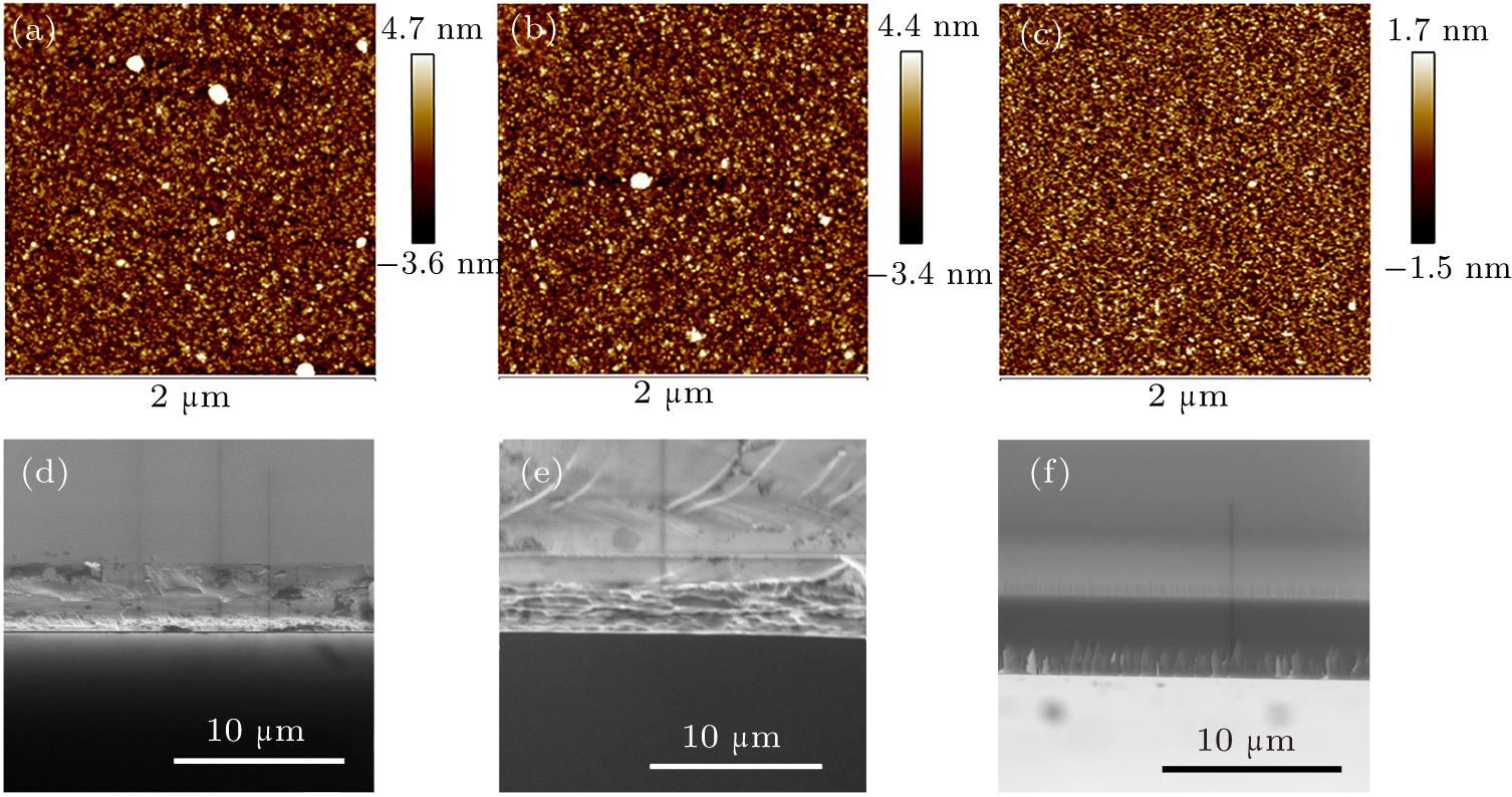
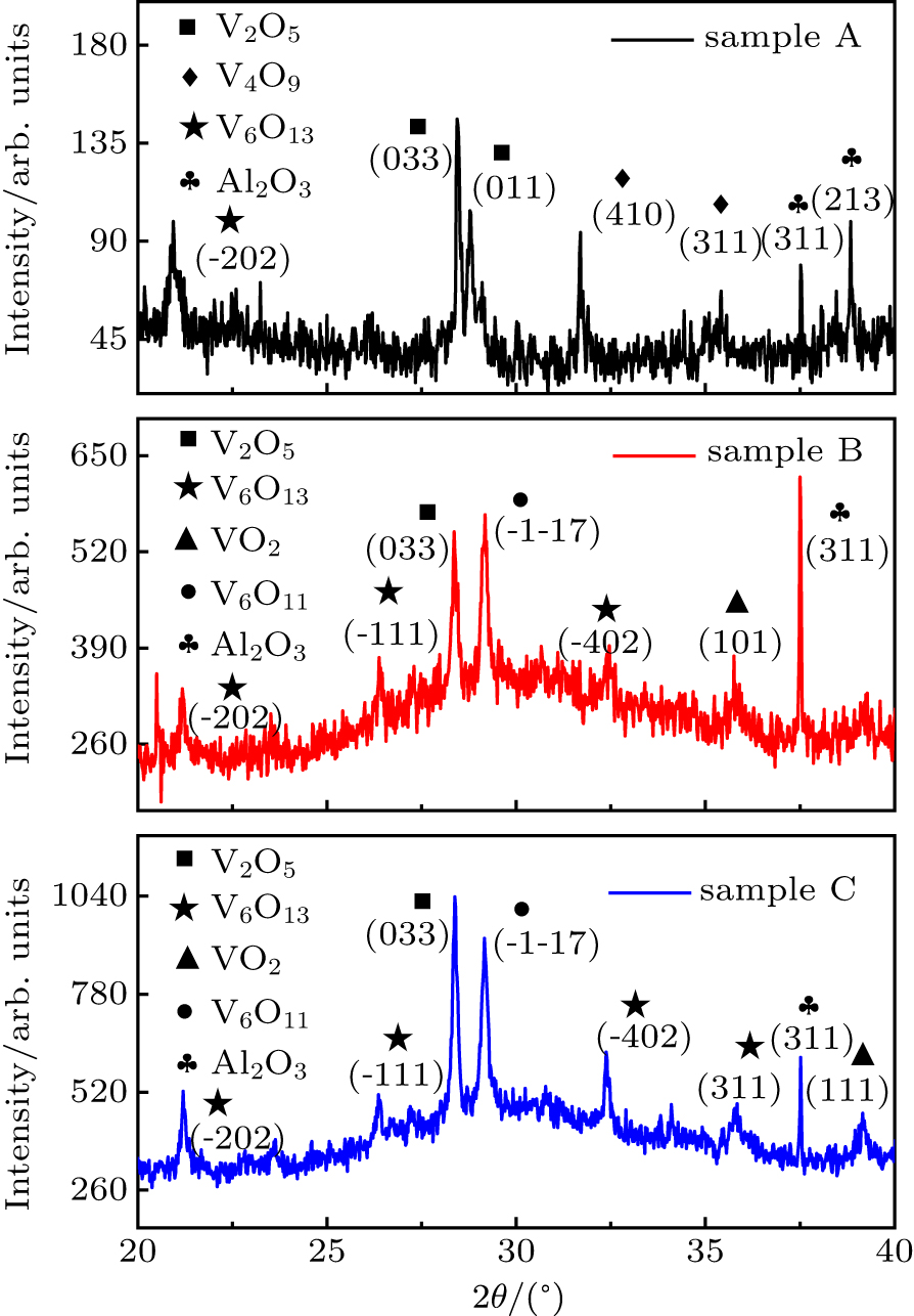
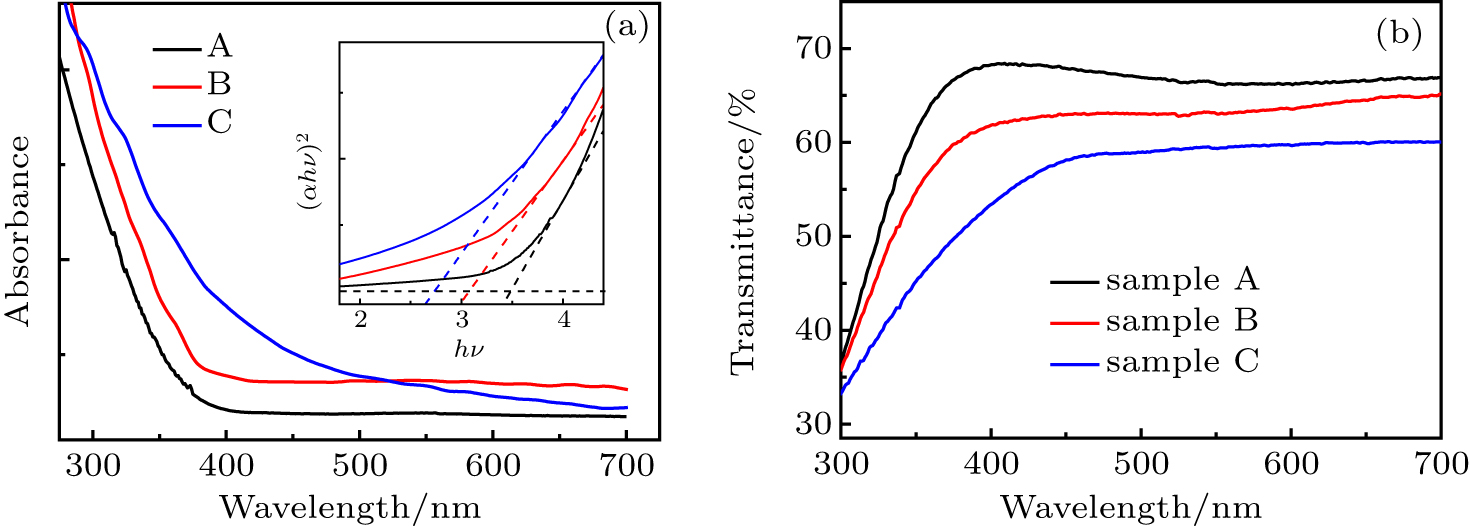
Abstract  

Vanadium oxide films were grown by atomic layer deposition using the tetrakis[ethylmethylamino] vanadium as the vanadium precursor and H2O as the oxide source. The effect of the source temperature on the quality of vanadium oxide films and valence state was investigated. The crystallinity, surface morphology, film thickness, and photoelectric properties of the films were characterized by x-ray diffraction, atomic force microscope, scanning electron microscope, IV characteristics curves, and UV–visible spectrophotometer. By varying the source temperature, the content of V6O11, VO2, and V6O13 in the vanadium oxide film increased, that is, as the temperature increased, the average oxidation state generally decreased to a lower value, which is attributed to the rising of the vapor pressure and the change of the ionization degree for organometallics. Meanwhile, the root-mean-square roughness decreased and the metal–insulator transition temperature reduced. Our study is great significance for the fabrication of vanadium oxide films by atomic layer deposition.

Keywords:  vanadium oxide films      atomic layer deposition      source temperature      valence state  
Received:  16 January 2020      Revised:  30 July 2020      Accepted manuscript online:  13 August 2020
PACS:  71.30.+h (Metal-insulator transitions and other electronic transitions)  
  61.50.Nw (Crystal stoichiometry)  
  61.05.cp (X-ray diffraction)  
Corresponding Authors:  Corresponding author. E-mail: wccwss@foxmail.com Corresponding author. E-mail: zpweicust@126.com   
About author: 
†Corresponding author. E-mail: wccwss@foxmail.com
‡Corresponding author. E-mail: zpweicust@126.com
* Project supported by the National Natural Science Foundation of China (Grant Nos. 11674038, 61674021, 61704011, and 61904017), the Developing Project of Science and Technology of Jilin Province, China (Grant Nos. 20170520118JH and 20160520027JH), and the Youth Foundation of Changchun University of Science and Technology (Grant No. XQNJJ-2018-18).

Cite this article: 

Bingheng Meng(孟兵恒), Dengkui Wang(王登魁)†, Deshuang Guo(郭德双), Juncheng Liu(刘俊成), Xuan Fang(方铉), Jilong Tang(唐吉龙), Fengyuan Lin(林逢源), Xinwei Wang(王新伟), Dan Fang(房丹), and Zhipeng Wei(魏志鹏)‡ Effect of source temperature on phase and metal–insulator transition temperature of vanadium oxide films grown by atomic layer deposition 2020 Chin. Phys. B 29 107102

Fig. 1.  

(a)–(c) The AFM images of samples A–C. (d)–(f) The SEM micrographs in cross-sectional view of samples A–C.

Fig. 2.  

The XRD pattern of VOx films deposited on sapphire substrate with different source temperatures: (a) 90 °C, (b) 100 °C, and (c) 110 °C.

Source temperature/°C IV2O5 / IAl2O3 IV4O9 / IAl2O3 IV6O13 / IAl2O3 IVO2 / IAl2O3 IV6O11 / IAl2O3
90 3.09 2.24 1.91 0 0
100 3.51 0 1.08 1.37 3.57
110 7.27 0 2.31 3.86 10.12
Table 1.  

Variation of the ratio of the strongest integrated intensity of each vanadium oxide in the film to the strongest integrated intensity of the substrate peak with the source temperature.

Fig. 3.  

(a) The absorption spectra and (b) transmission spectra of samples A–C.

Fig. 4.  

The relation of conductivity and temperature. The insets show the IV curves at 30 °C and 208 °C for samples A–C.

[1]
Yang Z, Ko C, Ramanathan S 2011 Annu. Rev. Mater. Res. 41 337 DOI: 10.1146/annurev-matsci-062910-100347
[2]
Cui Y Y, Ke Y J, Liu C, Chen Z, Wang N, Zhang L M, Zhou Y, Wang S C, Ga Y F, Long Y 2018 Joule 2 1 DOI: 10.1016/j.joule.2017.10.014
[3]
Shao Z W, Cao X, Zhang Q X, Long S W, Chang T C, Xu F, Yang Y, Jin P 2019 Sol. Energ. Mater. Sol. C 200 110044 DOI: 10.1016/j.solmat.2019.110044
[4]
Xu F, Cao X, Luo H, Jin P 2018 J. Mater. Chem. C 6 1903 DOI: 10.1039/C7TC05768G
[5]
Son M, Lee J, Park J, Shin J, Choi G, Jung S, Lee W, Kim S, Park S, Hwang H 2011 IEEE Electr. Device L. 32 1579 DOI: 10.1109/LED.2011.2163697
[6]
Wang Z L, Zhang Z H, Zhao Z, Shao R W, Sui M L 2018 Acta Phys. Sin. 67 177201 in Chinese DOI: 10.7498/aps.67.177201
[7]
Sun X N, Qu Z M, Wang Q G, Yuan Y, Liu S H 2019 Acta Phys. Sin. 68 107201 in Chinese DOI: 10.7498/aps.68.107201
[8]
Chen X Y, Pomerantseva E, Banerjee P, Gregorczyk K, Ghodssi R, Rubloff G 2012 Chem. Mater. 24 1255 DOI: 10.1021/cm202901z
[9]
Schwingenschlögl U, Eyert V, Eckern U 2003 Euro Phy. Lett. 61 361 DOI: 10.1209/epl/i2003-00182-9
[10]
Shin S, Suga S, Taniguchi M, Fujisawa M, Kanzaki H, Fujimori A, Daimon H, Ueda Y, Kosuge K, Kachi S 1990 Phys. Rev. B 41 4993 DOI: 10.1103/PhysRevB.41.4993
[11]
Raja S, Subramani G, Bheeman D, Rajamani R, Bellan C 2016 Optik 127 461 DOI: 10.1016/j.ijleo.2015.08.045
[12]
Wriedt H A 1989 Bull. Alloy Phase Diagrams 10 271 DOI: 10.1007/BF02877512
[13]
Chiu T W, Tonooka K, Kikuchi N 2010 Thin Solid Films 518 7441 DOI: 10.1016/j.tsf.2010.05.019
[14]
Nandakumar N K, Seebauer E G 2011 Thin Solid Films 519 3663 DOI: 10.1016/j.tsf.2011.02.002
[15]
Hanlon T J, Walker R E, Coath J A, Richardson M A 2002 Thin Solid Films 405 234 DOI: 10.1016/S0040-6090(01)01753-9
[16]
Yun S J, Lim J W, Noh J S, Chae B G, Kim H T 2008 Jpn. J. Appl. Phys. 47 3067 DOI: 10.1143/JJAP.47.3067
[17]
Subrahmanyam A, Reddy Y B K, Nagendra C L 2008 J. Phys. D: Appl. Phys. 41 195108 DOI: 10.1088/0022-3727/41/19/195108
[18]
Blanquart T, Niinistö J, Gavagnin M, Longo V, Heikkilä M, Puukilainen E, Pallem V R, Dussarrat C, Ritala M, Leskelä M 2013 RSC Adv. 3 1179 DOI: 10.1039/C2RA22820C
[19]
Rampelberg G, Deduytsche D, Schutter B D, Premkumar P A, Toeller M, Schaekers M, Martens K, Radu I, Detavernier C 2014 Thin Solid Films 550 59 DOI: 10.1016/j.tsf.2013.10.039
[20]
Griffiths C H, Eastwood H K 1974 J. Appl. Phys. 45 2201 DOI: 10.1063/1.1663568
[21]
Monnier D, Nuta I, Chatillon C, Gros-Jean M, Volpi F, Blanquet E 2009 J. Electrochem. Soc. 156 H71 DOI: 10.1149/1.3009595
[22]
Mattelaer F, Geryl K, Rampelberg G, Dobbelaere T, Dendooven J, Detavernier C 2016 RSC Adv. 6 114658 DOI: 10.1039/C6RA25742A
[23]
Van Heerden J L, Swanepoel R 1997 Thin Solid Films 299 72 DOI: 10.1016/S0040-6090(96)09281-4
[24]
Criado M, Fernández-Jiménez A, de la Torre A G, Aranda M A G, Palomo A 2007 Cem. Concr. Res. 37 671 DOI: 10.1016/j.cemconres.2007.01.013
[25]
Li W, Wang D K, Zhang Z Z, Chu X Y, Fang X, Wang X W, Fang D, Lin F Y, Wang X H, Wei Z P 2018 Opt. Mater. Express 8 3561 DOI: 10.1364/OME.8.003561
[26]
Goodenough J B 1971 J. Solid State Chem. 3 490 DOI: 10.1016/0022-4596(71)90091-0
[1] Physical analysis of normally-off ALD Al2O3/GaN MOSFET with different substrates using self-terminating thermal oxidation-assisted wet etching technique
Cheng-Yu Huang(黄成玉), Jin-Yan Wang(王金延), Bin Zhang(张斌), Zhen Fu(付振), Fang Liu(刘芳), Mao-Jun Wang(王茂俊), Meng-Jun Li(李梦军), Xin Wang(王鑫), Chen Wang(汪晨), Jia-Yin He(何佳音), and Yan-Dong He(何燕冬). Chin. Phys. B, 2022, 31(9): 097401.
[2] Designing high k dielectric films with LiPON—Al2O3 hybrid structure by atomic layer deposition
Ze Feng(冯泽), Yitong Wang(王一同), Jilong Hao(郝继龙), Meiyi Jing(井美艺), Feng Lu(卢峰), Weihua Wang(王维华), Yahui Cheng(程雅慧), Shengkai Wang(王盛凯), Hui Liu(刘晖), and Hong Dong(董红). Chin. Phys. B, 2022, 31(5): 057701.
[3] Uniform light emission from electrically driven plasmonic grating using multilayer tunneling barriers
Xiao-Bo He(何小波), Hua-Tian Hu(胡华天), Ji-Bo Tang(唐继博), Guo-Zhen Zhang(张国桢), Xue Chen(陈雪), Jun-Jun Shi(石俊俊), Zhen-Wei Ou(欧振伟), Zhi-Feng Shi(史志锋), Shun-Ping Zhang(张顺平), Chang Liu(刘昌), and Hong-Xing Xu(徐红星). Chin. Phys. B, 2022, 31(1): 017803.
[4] Characterization and application in XRF of HfO2-coated glass monocapillary based on atomic layer deposition
Yan-Li Li(李艳丽), Ya-Bing Wang(王亚冰), Wei-Er Lu(卢维尔), Xiang-Dong Kong(孔祥东), Li Han(韩立), and Hui-Bin Zhao(赵慧斌). Chin. Phys. B, 2021, 30(5): 050703.
[5] Low-temperature plasma enhanced atomic layer deposition of large area HfS2 nanocrystal thin films
Ailing Chang(常爱玲), Yichen Mao(毛亦琛), Zhiwei Huang(黄志伟), Haiyang Hong(洪海洋), Jianfang Xu(徐剑芳), Wei Huang(黄巍), Songyan Chen(陈松岩), Cheng Li(李成). Chin. Phys. B, 2020, 29(3): 038102.
[6] Surface termination effects on the electrical characteristics of La2O3/Al2O3 nanolaminates deposited by atomic layer deposition
Ji-Bin Fan(樊继斌), Shan-Ya Ling(凌山雅), Hong-Xia Liu(刘红侠), Li Duan(段理), Yan Zhang(张研), Ting-Ting Guo(郭婷婷), Xing Wei(魏星), and Qing He(何清)$. Chin. Phys. B, 2020, 29(11): 117701.
[7] Formation of unusual Cr5+ charge state in CaCr0.5Fe0.5O3 perovskite
Jian-Hong Dai(戴建洪), Qing Zhao(赵庆), Qian Sun(孙倩), Shuo Zhang(张硕), Xiao Wang(王潇), Xu-Dong Shen(申旭东), Zhe-Hong Liu(刘哲宏), Xi Shen(沈希), Ri-Cheng Yu(禹日成), Ting-Shan Chan(詹丁山), Lun-Xiong Li(李论雄), Guang-Hui Zhou(周光辉), Yi-feng Yang(杨义峰), Chang-Qing Jin(靳常青), You-Wen Long(龙有文). Chin. Phys. B, 2018, 27(3): 037503.
[8] Crystalline silicon surface passivation investigated by thermal atomic-layer-deposited aluminum oxide
Cai-Xia Hou(侯彩霞), Xin-He Zheng(郑新和), Rui Jia(贾锐), Ke Tao(陶科), San-Jie Liu(刘三姐), Shuai Jiang(姜帅), Peng-Fei Zhang(张鹏飞), Heng-Chao Sun(孙恒超), Yong-Tao Li(李永涛). Chin. Phys. B, 2017, 26(9): 098103.
[9] Influences of different oxidants on characteristics of La2O3/Al2O3 nanolaminates deposited by atomic layer deposition
Ji-Bin Fan(樊继斌), Hong-Xia Liu(刘红侠), Li Duan(段理), Yan Zhang(张研), Xiao-Chen Yu(于晓晨). Chin. Phys. B, 2017, 26(6): 067701.
[10] Performance and reliability improvement of La2O3/Al2O3 nanolaminates using ultraviolet ozone post treatment
Ji-Bin Fan(樊继斌), Hong-Xia Liu(刘红侠), Bin Sun(孙斌), Li Duan(段理), Xiao-Chen Yu(于晓晨). Chin. Phys. B, 2017, 26(5): 057702.
[11] Influences of different structures on the characteristics of H2O-based and O3-based LaxAlyO films deposited by atomic layer deposition
Chen-Xi Fei(费晨曦), Hong-Xia Liu(刘红侠), Xing Wang(汪星), Dong-Dong Zhao(赵冬冬), Shu-Long Wang(王树龙), Shu-Peng Chen(陈树鹏). Chin. Phys. B, 2016, 25(5): 058106.
[12] Growth mechanism of atomic-layer-deposited TiAlC metal gatebased on TiCl4 and TMA precursors
Jinjuan Xiang(项金娟), Yuqiang Ding(丁玉强), Liyong Du(杜立永), Junfeng Li(李俊峰),Wenwu Wang(王文武), Chao Zhao(赵超). Chin. Phys. B, 2016, 25(3): 037308.
[13] A-site ordered perovskiteCaCu3Cu2Ir2O12-δ with square-planar and octahedral coordinated Cu ions
Qing Zhao(赵庆), Yun-Yu Yin(殷云宇), Jian-Hong Dai(戴建洪), Xi Shen(沈希), Zhi-Wei Hu(胡志伟), Jun-Ye Yang(杨俊叶), Qing-Tao Wang(王清涛), Ri-Cheng Yu(禹日成), Xiao-Dong Li(李晓东), You-Wen Long(龙有文). Chin. Phys. B, 2016, 25(2): 020701.
[14] Influences of annealing on structural and compositional properties of Al2O3 thin films grown on 4H-SiC by atomic layer deposition
Li-Xin Tian(田丽欣), Feng Zhang(张峰), Zhan-Wei Shen(申占伟), Guo-Guo Yan(闫果果), Xing-Fang Liu(刘兴昉), Wan-Shun Zhao(赵万顺), Lei Wang(王雷), Guo-Sheng Sun(孙国胜), Yi-Ping Zeng(曾一平). Chin. Phys. B, 2016, 25(12): 128104.
[15] Atomic-layer-deposited Al2O3 and HfO2 on InAlAs: A comparative study of interfacial and electrical characteristics
Li-Fan Wu(武利翻), Yu-Ming Zhang(张玉明), Hong-Liang Lv(吕红亮), Yi-Men Zhang(张义门). Chin. Phys. B, 2016, 25(10): 108101.
No Suggested Reading articles found!