| CONDENSED MATTER: ELECTRONIC STRUCTURE, ELECTRICAL, MAGNETIC, AND OPTICAL PROPERTIES |
Prev
Next
|
|
|
Interface and border trapping effects in normally-off Al2O3/AlGaN/GaN MOS-HEMTs with different post-etch surface treatments |
| Si-Qi Jing(荆思淇)1,2, Xiao-Hua Ma(马晓华)2, Jie-Jie Zhu(祝杰杰)1,2,†, Xin-Chuang Zhang(张新创)1,2, Si-Yu Liu(刘思雨)1,2, Qing Zhu(朱青)1,2, and Yue Hao(郝跃)2 |
1 School of Advanced Materials and Nanotechnology, Xidian University, Xi’an 710071, China
2 Key Laboratory of Wide Bandgap Semiconductor Technology, Xidian University, Xi’an 710071, China |
|
|
|
|
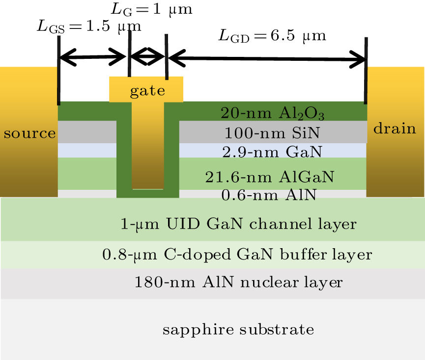
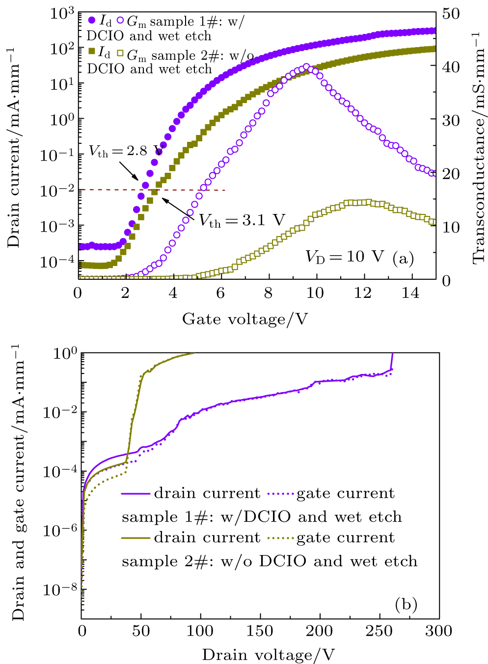
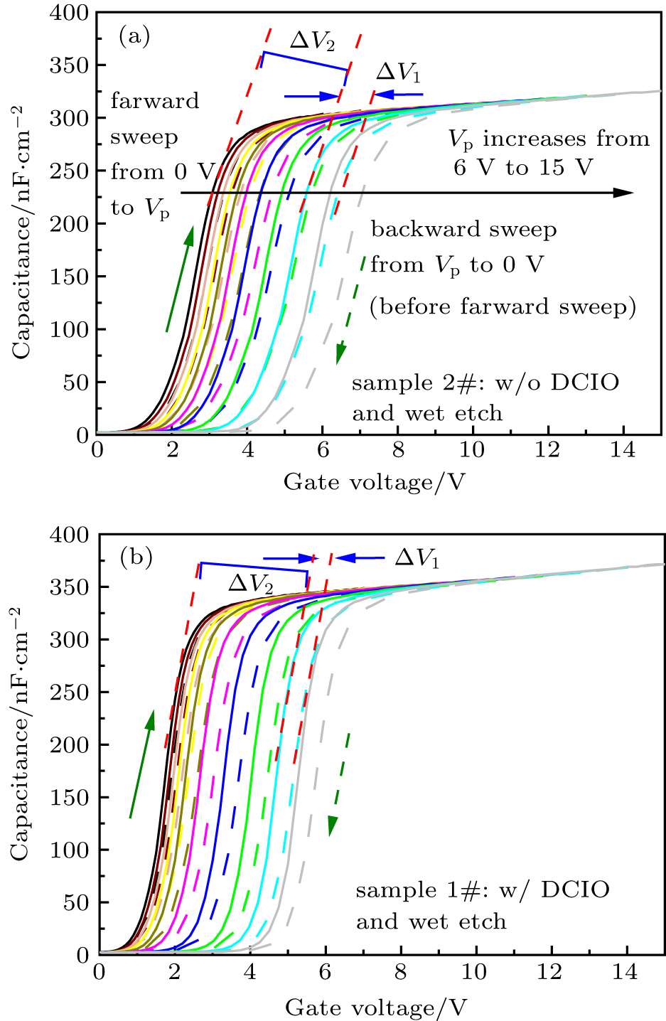
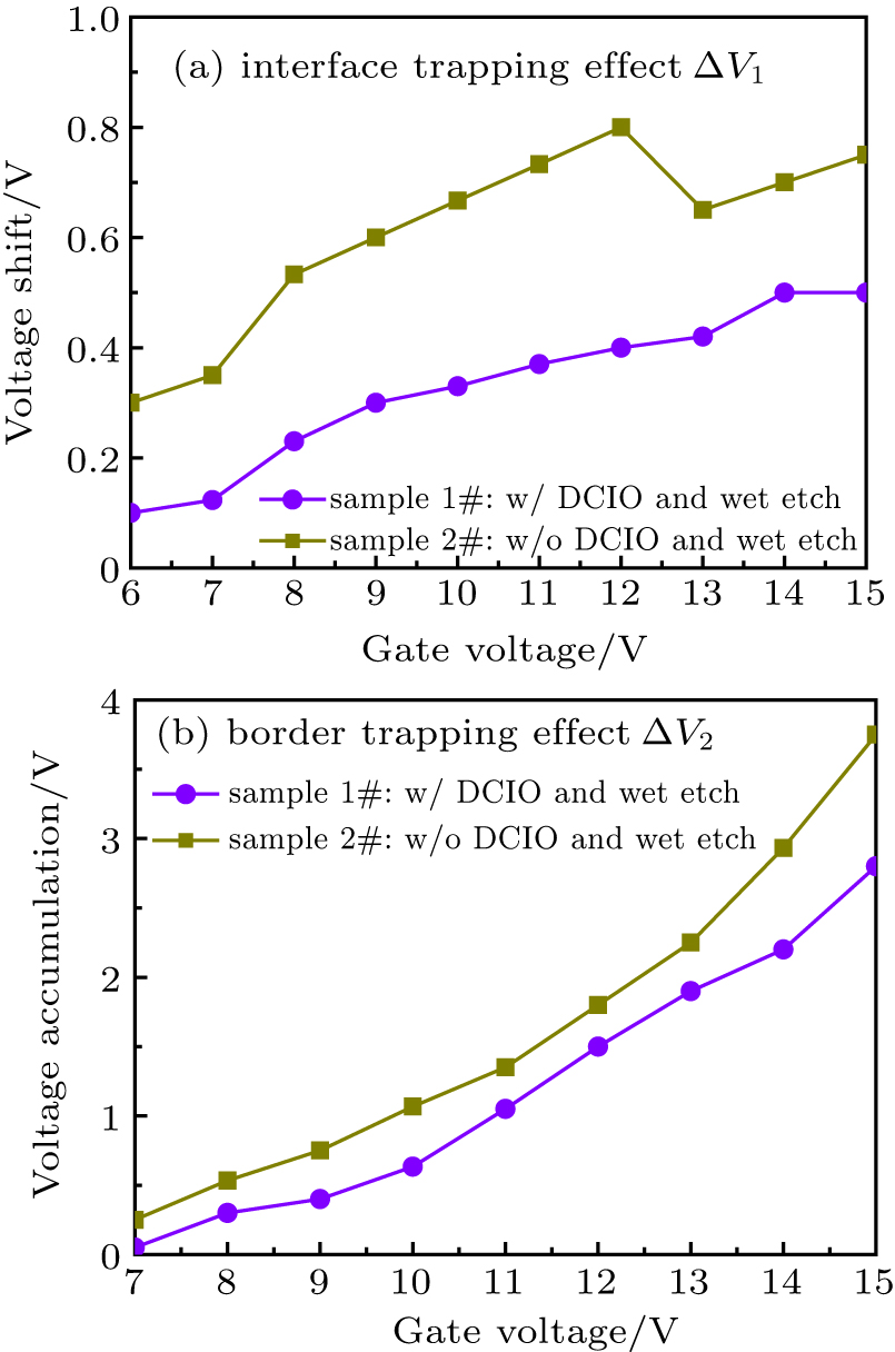
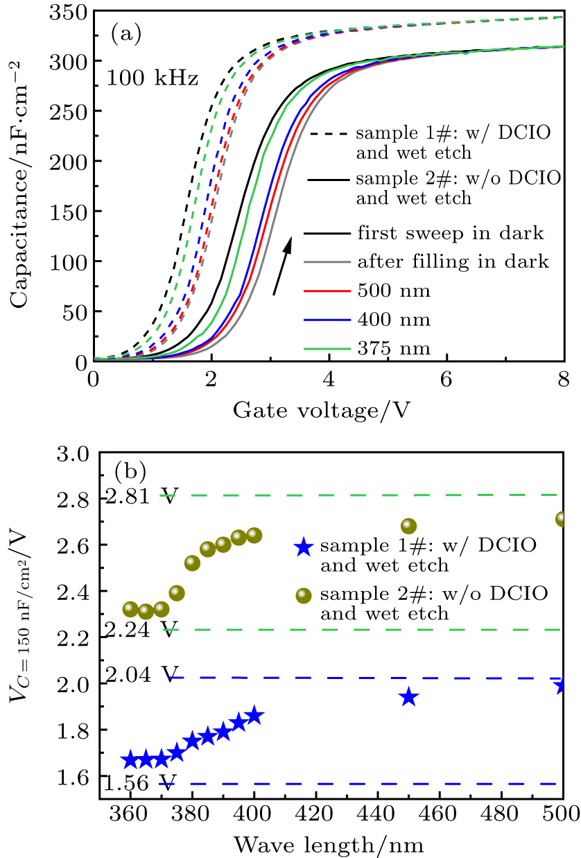
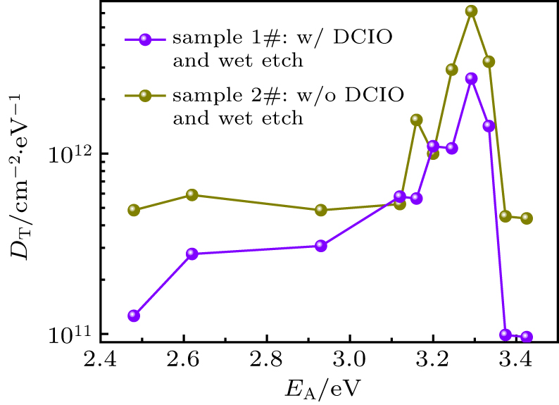
Abstract Trapping effect in normally-off Al2O3/AlGaN/GaN metal–oxide–semiconductor (MOS) high-electron-mobility transistors (MOS-HEMTs) with post-etch surface treatment was studied in this paper. Diffusion-controlled interface oxidation treatment and wet etch process were adopted to improve the interface quality of MOS-HEMTs. With capacitance–voltage (C–V) measurement, the density of interface and border traps were calculated to be 1.13 × 1012 cm−2 and 6.35 × 1012 cm−2, effectively reduced by 27% and 14% compared to controlled devices, respectively. Furthermore, the state density distribution of border traps with large activation energy was analyzed using photo-assisted C–V measurement. It is found that irradiation of monochromatic light results in negative shift of C–V curves, which indicates the electron emission process from border traps. The experimental results reveals that the major border traps have an activation energy about 3.29 eV and the change of post-etch surface treatment process has little effect on this major activation energy.
|
Received: 24 April 2020
Revised: 01 June 2020
Accepted manuscript online: 05 June 2020
|
|
PACS:
|
73.61.Ey
|
(III-V semiconductors)
|
| |
73.40.Qv
|
(Metal-insulator-semiconductor structures (including semiconductor-to-insulator))
|
| |
73.50.Gr
|
(Charge carriers: generation, recombination, lifetime, trapping, mean free paths)
|
|
|
Corresponding Authors:
†Corresponding author. E-mail: jjzhu@mail.xidian.edu.cn
|
| About author: †Corresponding author. E-mail: jjzhu@mail.xidian.edu.cn * Project supported by the National Natural Science Foundation of China (Grant Nos. 61704124, 11690042, and 61634005). |
Cite this article:
Si-Qi Jing(荆思淇), Xiao-Hua Ma(马晓华), Jie-Jie Zhu(祝杰杰)†, Xin-Chuang Zhang(张新创), Si-Yu Liu(刘思雨), Qing Zhu(朱青), and Yue Hao(郝跃) Interface and border trapping effects in normally-off Al2O3/AlGaN/GaN MOS-HEMTs with different post-etch surface treatments 2020 Chin. Phys. B 29 107302
|
| [1] |
|
| [2] |
Hou B, Ma X H, Yang L, Zhu J J, Zhu Q, Chen L X, Mi M H, Zhang H S, Zhang M, Zhang P, Zhou X W, Hao Y 2017 Appl. Phys. Express 10 076501 DOI: 10.7567/APEX.10.076501 |
| [3] |
Zheng X F, Wang A C, Hou X H, Wang Y Z, Wen H Y, Wang C, Lu Y, Mao W, Ma X H, Hao Y 2017 Chin. Phys. Lett. 34 27301 DOI: 10.1088/0256-307X/34/2/027301 |
| [4] |
|
| [5] |
Roberts J W, Chalker P R, Lee K B, Houston P A, Cho S J, Thayne I G, Guiney I, Wallis D, Humphreys C J 2016 Appl. Phys. Lett. 108 072901 DOI: 10.1063/1.4942093 |
| [6] |
Hou B, Ma X H, Zhu J J, Yang L, Chen W W, Mi M H, Zhu Q, Chen L X, Zhang R, Zhang M, Zhou X W, Hao Y 2018 IEEE Electron Dev. Lett. 39 397 DOI: 10.1109/LED.2018.2791441 |
| [7] |
Mochizuki K, Mishima T, Terano A, Kaneda N, Ishigaki T, Tsuchiya T 2011 IEEE Trans. Electron. Dev. 58 1979 DOI: 10.1109/TED.2011.2145380 |
| [8] |
Liu Z H, Ng G I, Arulkumaran S, Maung Y K T, Teo K L, Foo S C, Sahmugan-athan V 2009 Appl. Phys. Lett. 95 223501 DOI: 10.1063/1.3268474 |
| [9] |
Ma X H, Zhu J J, Liao X Y, Yue T, Chen W W, Hao Y 2013 Appl. Phys. Lett. 103 033510 DOI: 10.1063/1.4813912 |
| [10] |
Zhou Q, Liu L, Zhang A B, Chen B W, Jin Y, Shi Y Y, Wang Z H, Chen W J, Zhang B 2016 IEEE Electron Dev. Lett. 37 165 DOI: 10.1109/LED.2015.2511026 |
| [11] |
Sang F, Wang M J, Tao M, Liu S F, Yu M, Xie B, Wen C P, Wang J Y, Wu W G, Hao Y L, Shen B 2016 Appl. Phys. Express 9 091001 DOI: 10.7567/APEX.9.091001 |
| [12] |
Zhu J J, Zhu Q, Chen L X, Hou B, Yang L, Zhou X W, Ma X H, Hao Y 2017 IEEE Trans. Electron. Dev. 64 840 DOI: 10.1109/TED.2017.2657780 |
| [13] |
Wang M J, Wang Y, Zhang C, Xie B, Wen C P, Wang J Y, Hao Y L, Wu W G, Chen K J, Shen B 2014 IEEE Trans. Electron. Dev. 61 2035 DOI: 10.1109/TED.2014.2315994 |
| [14] |
Fleetwood D M, Winokur P S, Reber J R A, Meisenheimer T L, Schwank J R, Shaneyfelt M R, Riewe L C 1993 J. Appl. Phys. 73 5058 DOI: 10.1063/1.353777 |
| [15] |
|
| [16] |
Zhu J J, Ma X H, Hou B, Ma M, Zhu Q, Chen L X, Yang L, Zhang P, Zhou X W, Hao Y 2018 IEEE Trans. Electron. Dev. 65 5343 DOI: 10.1109/TED.2018.2874314 |
| [17] |
Yang S, Tang Z K, Wong K Y, Lin Y S, Liu C, Lu Y Y, Huang S, Chen K J 2013 IEEE Electron Dev. Lett. 34 1497 DOI: 10.1109/LED.2013.2286090 |
| [18] |
Partida-Manzanera T, Zaid Z H, Roberts J W, Dolmanan S B, Lee K B, Houston P A, Chalker P R, Tripathy S, Potter R J 2019 J. Appl. Phys. 126 034102 DOI: 10.1063/1.5049220 |
| [19] |
Zhu J J, Ma M, Zhu Q, Hou B, Chen L X, Yang L, Zhou X W, Ma X H, Hao Y 2018 2018 IEEE Workshop on Wide Bandgap Power Devices and Applications in Asia WiPDA Asia May 17–19, 2018 Xi’an, China 135 DOI: 10.1109/WiPDAAsia.2018.8734573 |
| [20] |
Zhu J J, Zhang Y C, Ma X H, Liu S Y, Jing S Q, Zhu Q, Mi M H, Hou B, Yang L, Uren M J, Kuball M, Hao Y 2020 Semiconductor Science and Technology 35 065017 DOI: 10.1088/1361-6641/ab8356 |
| [21] |
Sun H, Wang M J, Yin R Y, Chen J G, Xue S, Luo J S, Hao Y L, Chen D M 2019 IEEE Trans. Electron. Dev. 66 3290 DOI: 10.1109/TED.16 |
| [22] |
|
| [23] |
Zheng X F, Dong S S, Ji P, Wang C, He Y L, Lv L, Ma X H, Hao Y 2018 Appl. Phys. Lett. 112 233504 DOI: 10.1063/1.5024645 |
| [24] |
Liu S H, Yang S, Tang Z K, Jiang Q M, Liu C, Wang M J, Shen B, Chen K J 2015 Appl. Phys. Lett. 106 051605 DOI: 10.1063/1.4907861 |
| [25] |
Qin X Y, Lucero A, Azcatl A, Kim J, Wallace R M 2014 Appl. Phys. Lett. 105 011602 DOI: 10.1063/1.4887056 |
| [26] |
Zhou X Y, Lv Y J, Tan X, Wang Y G, Song X B, He Z Z, Zhang Z R, Liu Q B, Han T T, Fang Y L, Feng Z H 2018 Acta Phys. Sin. 67 178501 in Chinese DOI: 10.7498/aps.67.20180474 |
| [27] |
|
| [28] |
Shen Z, He L, Zhou G L, Yao Y, Yang F, Ni Y Q, Zheng Y, Zhou D Q, Ao J P, Zhang B J, Liu Y 2016 Phys. Status Solidi 213 2693 DOI: 10.1002/pssa.201532785 |
| [29] |
Yatabe Z, Hori Y, Ma W C, Asubar J T, Akazawa M, Sato T, Hashizume T 2014 J. Appl. Phys. 53 100213 DOI: 10.7567/JJAP.53.100213 |
| No Suggested Reading articles found! |
|
|
Viewed |
|
|
|
Full text
|
|
|
|
|
Abstract
|
|
|
|
|
Cited |
|
|
|
|
Altmetric
|
|
blogs
Facebook pages
Wikipedia page
Google+ users
|
Online attention
Altmetric calculates a score based on the online attention an article receives. Each coloured thread in the circle represents a different type of online attention. The number in the centre is the Altmetric score. Social media and mainstream news media are the main sources that calculate the score. Reference managers such as Mendeley are also tracked but do not contribute to the score. Older articles often score higher because they have had more time to get noticed. To account for this, Altmetric has included the context data for other articles of a similar age.
View more on Altmetrics
|
|
|