Please wait a minute...
Chin. Phys. B, 2020, Vol. 29(10): 107201    DOI: 10.1088/1674-1056/abaed8
CONDENSED MATTER: ELECTRONIC STRUCTURE, ELECTRICAL, MAGNETIC, AND OPTICAL PROPERTIES Prev   Next  

Evaluation of stress voltage on off-state time-dependent breakdown for GaN MIS-HEMT with SiNx gate dielectric

Tao-Tao Que(阙陶陶)1, Ya-Wen Zhao(赵亚文)1, Qiu-Ling Qiu(丘秋凌)1, Liu-An Li(李柳暗)1, Liang He(何亮)2, Jin-Wei Zhang(张津玮)1, Chen-Liang Feng(冯辰亮)1, Zhen-Xing Liu(刘振兴)1, Qian-Shu Wu(吴千树)1, Jia Chen(陈佳)1, Cheng-Lang Li(黎城朗)1, Qi Zhang(张琦)1, Yun-Liang Rao(饶运良)1, Zhi-Yuan He(贺致远)3, and Yang Liu (刘扬)1,
1 School of Electronics and Information Technology, Sun Yat-Sen University, Guangzhou 510275, China
2 School of Materials Science and Engineering, Sun Yat-Sen University, Guangzhou 510275, China
3 Science and Technology on Reliability Physics and Application of Electronic Component Laboratory, No. 5 Electronics Research Institute of the Ministry of Industry and Information Technology, Guangzhou 510610, China
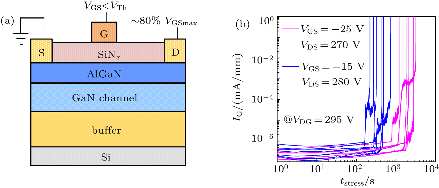
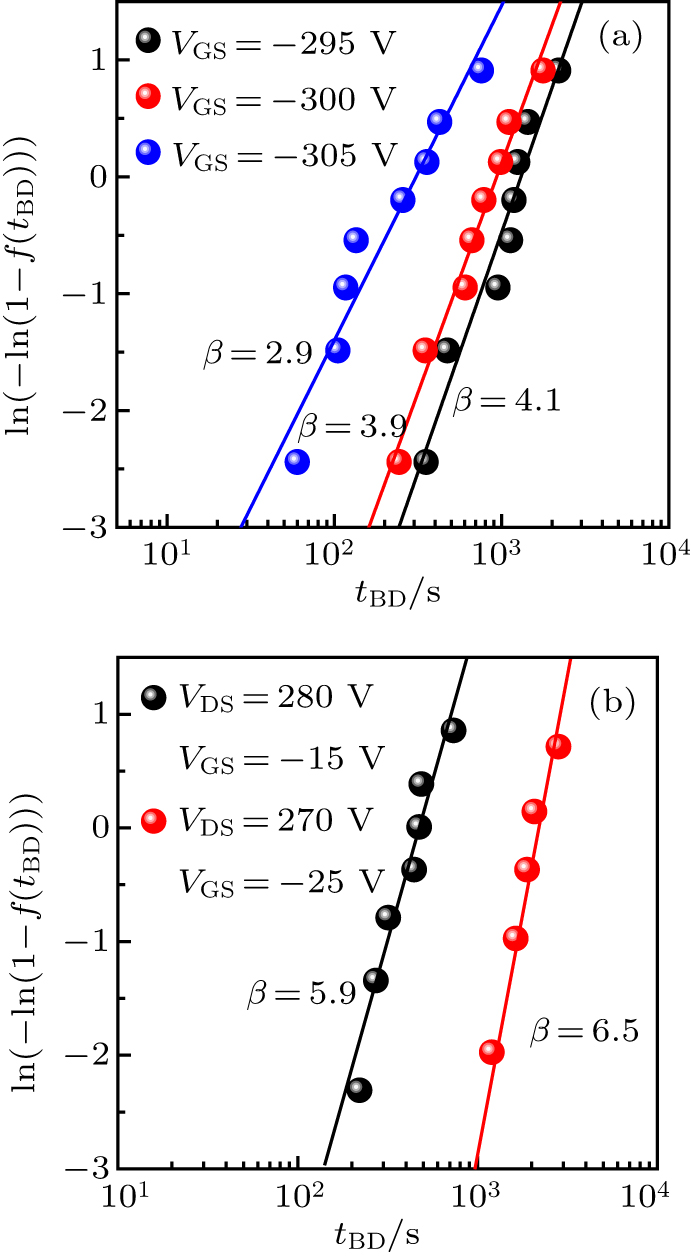
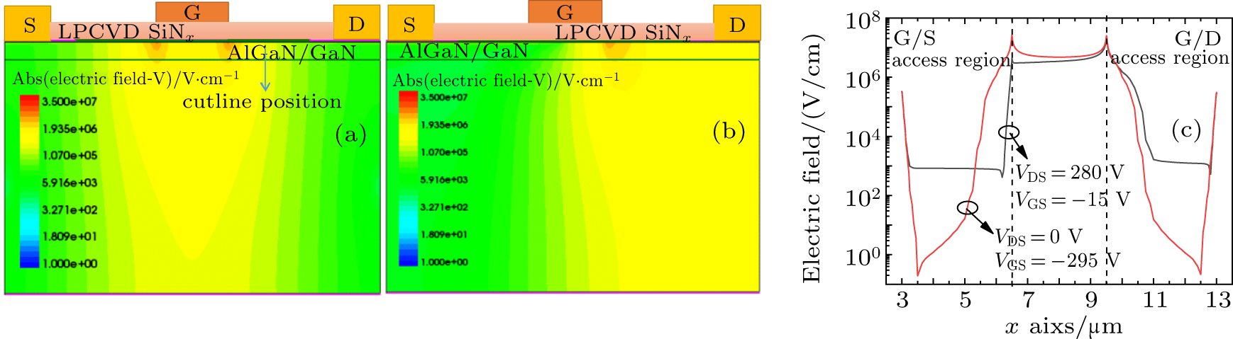
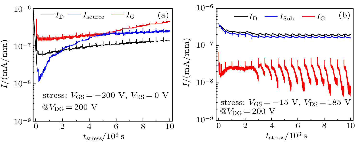
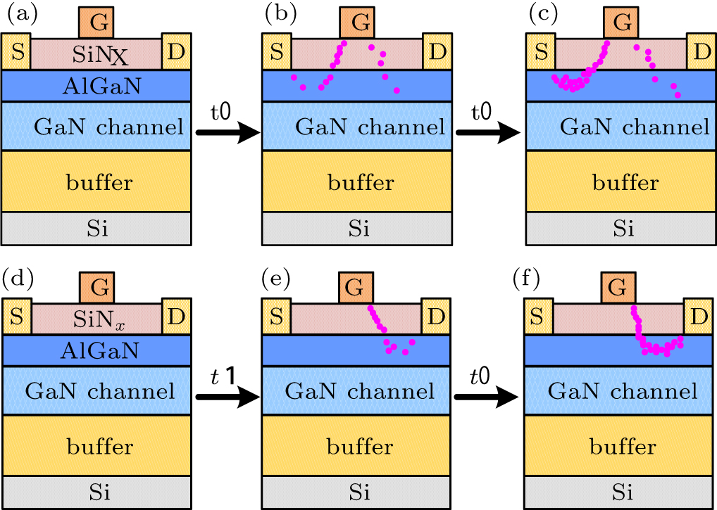
Abstract  

Stress voltages on time-dependent breakdown characteristics of GaN MIS-HEMTs during negative gate bias stress (with VGS < 0, VD = VS = 0) and off-state stress (VG < VTh, VDS > 0, VS = 0) are investigated. For negative bias stress, the breakdown time distribution (β) decreases with the increasing negative gate voltage, while β is larger for higher drain voltage at off-state stress. Two humps in the time-dependent gate leakage occurred under both breakdown conditions, which can be ascribed to the dielectric breakdown triggered earlier and followed by the GaN layer breakdown. Combining the electric distribution from simulation and long-term monitoring of electric parameter, the peak electric fields under the gate edges at source and drain sides are confirmed as the main formation locations for per-location paths during negative gate voltage stress and off-state stress, respectively.

Keywords:  gallium nitride      LPCVD-SiNx MIS-HEMT      time-dependent breakdown      negative gate bias      offstate stress  
Received:  03 July 2020      Revised:  10 August 2020      Accepted manuscript online:  13 August 2020
PACS:  72.80.Ey (III-V and II-VI semiconductors)  
  72.80.Sk (Insulators)  
  73.20.At (Surface states, band structure, electron density of states)  
  77.22.Jp (Dielectric breakdown and space-charge effects)  
Corresponding Authors:  Corresponding author. E-mail: liuy69@mail.sysu.edu.cn   
About author: 
†Corresponding author. E-mail: liuy69@mail.sysu.edu.cn
* Project supported by the National Key Research and Development Program, China (Grant No. 2017YFB0402800), the Key Research and Development Program of Guangdong Province, China (Grant Nos. 2019B010128002 and 2020B010173001), the National Natural Science Foundation of China (Grant No. U1601210), the Natural Science Foundation of Guangdong Province, China (Grant No. 2015A030312011), the Open Project of Key Laboratory of Microelectronic Devices and Integrated Technology (Grant No. 202006), the Science and Technology Plan of Guangdong Province, China (Grant No. 2017B010112002), and the China Postdoctoral Science Foundation (Grant No. 2019M663233).

Cite this article: 

Tao-Tao Que(阙陶陶), Ya-Wen Zhao(赵亚文), Qiu-Ling Qiu(丘秋凌), Liu-An Li(李柳暗), Liang He(何亮), Jin-Wei Zhang(张津玮), Chen-Liang Feng(冯辰亮), Zhen-Xing Liu(刘振兴), Qian-Shu Wu(吴千树), Jia Chen(陈佳), Cheng-Lang Li(黎城朗), Qi Zhang(张琦), Yun-Liang Rao(饶运良), Zhi-Yuan He(贺致远), and Yang Liu (刘扬)† Evaluation of stress voltage on off-state time-dependent breakdown for GaN MIS-HEMT with SiNx gate dielectric 2020 Chin. Phys. B 29 107201

Fig. 1.  

(a) Transfer and (b) off-state blocking voltage characteristics of the GaN MIS-HEMT.

Fig. 2.  

(a) Test diagrams of negative bias stress and (b) time-dependent breakdown with VGS = −295 V, −300 V, −305 V, respectively, and (c) lifetime extrapolation for 20 years based on 1/E model with failure rate of 63.2% and 0.01%.

Fig. 3.  

(a) Test diagrams of off-state stress and (b) time-dependent breakdown during off-state stress with VDS = 280 V and VDS = 270 V @VDG = 295 V.

Fig. 4.  

(a) The comparison of time-dependent breakdown between negative gate voltage stress and off-state stress. (b) Two sudden increasing trends of gate leakage occur during both stress conditions.

Fig. 5.  

Breakdown time distribution (β) of (a) negative gate bias with VGS = −295 V, −300 V, −305 V, respectively and (b) off-state stress with VDS = 280 V and VDS = 270 V @VDG = 295 V.

Fig. 6.  

Simulation of electric field distribution for rapid breakdown under (a) negative bias stress @VDG = 295 V and (b) off-state stress @VDG = 295 V. (c) Extraction of electric field distribution at the cutline of 10 nm below SiNx/AlGaN interface for both of the two stress conditions.

Fig. 7.  

The evolution of threshold voltage and on resistance during stress and recovery conditions of VGS = −200 V, VDS = 0 V, and VGS = −15 V, VDS = 185 V @VDG = 200 V.

Fig. 8.  

The evolution of leakage during (a) negative gate bias at VGS = −200 V, VDS = 0 V @VDG = 295 V and (b) off-state stress at VGS = −15 V, VDS = 185 V @VDG = 200 V.

Fig. 9.  

The schematic mechanism for the negative bias stress (a)–(c) and off-state time-dependent breakdown process (e)–(g).

Fig. 10.  

Transfer characteristics and IGS before stress and after adequate recovery of (a) negative bias stress at VGS = −200 V, VDS = 0 V @VDG = 200 V and (b) off-state stress at VGS = −15 V, VDS = 185 V @VDG = 200 V.

[1]
Moens P, Liu C, Banerjee A, Vanmeerbeek P, Coppens P, Ziad H 2014 Proc. Int. Symp. Power Semicond. Dev. and ICs. 6 374 DOI: 10.1109/ispsd.2014.6856054
[2]
Li L, Zhang J, Liu Y, Ao J 2016 Chin. Phys. B 25 038503 DOI: 10.1088/1674-1056/25/3/038503
[3]
Hua M, Liu C, Yang S, Liu S, Fu K, Dong Z, Cai Y, Zhang B, Chen K 2015 IEEE Electron Device Lett. 36 448 DOI: 10.1109/LED.2015.2409878
[4]
Cook T, Fulton C, Mecouch W, Davis R, Namanich R 2003 Appl. Phys. 94 3949 DOI: 10.1063/1.1601314
[5]
Zhang Z, Qin S, Fu K, Yu G, Li W, Zhang X, Sun S, Song L, Li S, Hao R, Fan Y, Sun Q, Pan G, Cai Y, Zhang B 2016 Appl. Phys. Express 9 084102 DOI: 10.7567/APEX.9.084102
[6]
Hua M, Qian Q, Wei J, Zhang Z, Tang G, Chen K 2018 Physica Status Solidi (a) 215 1700641 DOI: 10.1002/pssa.v215.10
[7]
Hua M, Liu M, Yang S, Liu S, Fu K, Dong Z 2015 Trans. Electron Dev. 62 3215 DOI: 10.1109/TED.2015.2469716
[8]
del Alamo J, Guo A, Warnock S 2017 Journal of Materials Research 32 3458 DOI: 10.1557/jmr.2017.363
[9]
Meneghini M, Rossetto I, Bisi D, Ruzzarin M, Hove M, Stoffels S, Wu T, Marcon D, Decoutere S, Meneghesso G 2016 IEEE Electron Dev. Lett. 37 474 DOI: 10.1109/LED.2016.2530693
[10]
Marcon D, Meneghesso G, Wu T, Stoffels S, Meneghini M, Zanoni E, Decoutere S 2013 IEEE Trans. Electron Dev. 60 3132 DOI: 10.1109/TED.2013.2273216
[11]
Wamock S, del Alamo J 2017 IEEE IRPS 4 B-3-1 DOI: 10.1109/WiPDA46397.2019.8998949
[12]
Yang W, Yuan J, Krishnan B, Shea P 2019 IEEE 7th WiPDA 277 DOI: 10.1109/WiPDA46397.2019.8998949
[13]
Hua M, Wei J, Bao Q, Zhang Z, Zheng Z, Chen K 2015 IEEE Electron Dev. Lett. 39 413 DOI: 10.1109/LED.2018.2791664
[14]
Guo A, del Alamo J 2016 IEEE IRPS 4 A-1-1 DOI: 10.1109/IRPS.2016.7574526
[15]
Que T, Zhao Y, Li L, He L, Qiu Q, Liu Z, Zhang J, Chen J, Wu Z, Liu Y 2020 Chin. Phys. B 29 037201 DOI: 10.1088/1674-1056/ab696b
[16]
Song L, Fu K, Zhao J, Yu G, Hao R, Fan Y, Cai Y, Zhang B 2018 J. Vac. Sci. & Technol. B 36 042201 DOI: 10.1116/1.5023844
[17]
Qi Y, Zhu Y, Zhang J, Lin X, Cheng K, Jiang L, Yu H 2018 IEEE Trans. Electron Dev. 65 1759 DOI: 10.1109/TED.2018.2813985
[18]
Jauss S, Hallaceli K, Mansfeld S, Schwaiger S, Daves W, Ambacher O 2017 IEEE Trans. Electron Dev. 64 2298 DOI: 10.1109/TED.2017.2682931
[19]
Warnock S, del Alamo J 2016 IEEE IRPS 4 A-6-1 DOI: 10.1109/TED.2018.2813985
[20]
Warnock S, del Alamo J 2017 IEEE IRPS 4 B-3.1 DOI: 10.1088/1674-1056/ab8895
[21]
Degraeve R, Kaczer B, Groeseneken G 1999 Microelectronics Reliability 39 1445 DOI: 10.1016/S0026-2714(99)00051-7
[22]
Jin D, Joh J, Krishnan S, Tipirneni N, Pendharkar S, del Alamo J 2013 IEEE IEDM 6 2.1 DOI: 10.1109/ispsd.2014.6856054
[1] Review of a direct epitaxial approach to achieving micro-LEDs
Yuefei Cai(蔡月飞), Jie Bai(白洁), and Tao Wang(王涛). Chin. Phys. B, 2023, 32(1): 018508.
[2] Self-screening of the polarized electric field in wurtzite gallium nitride along [0001] direction
Qiu-Ling Qiu(丘秋凌), Shi-Xu Yang(杨世旭), Qian-Shu Wu(吴千树), Cheng-Lang Li(黎城朗), Qi Zhang(张琦), Jin-Wei Zhang(张津玮), Zhen-Xing Liu(刘振兴), Yuan-Tao Zhang(张源涛), and Yang Liu(刘扬). Chin. Phys. B, 2022, 31(4): 047103.
[3] Effect of heavy ion irradiation on the interface traps of AlGaN/GaN high electron mobility transistors
Zheng-Zhao Lin(林正兆), Ling Lü(吕玲), Xue-Feng Zheng(郑雪峰), Yan-Rong Cao(曹艳荣), Pei-Pei Hu(胡培培), Xin Fang(房鑫), and Xiao-Hua Ma(马晓华). Chin. Phys. B, 2022, 31(3): 036103.
[4] Protection of isolated and active regions in AlGaN/GaN HEMTs using selective laser annealing
Mingchen Hou(侯明辰), Gang Xie(谢刚), Qing Guo(郭清), and Kuang Sheng(盛况). Chin. Phys. B, 2021, 30(9): 097302.
[5] Modeling, simulations, and optimizations of gallium oxide on gallium-nitride Schottky barrier diodes
Tao Fang(房涛), Ling-Qi Li(李灵琪), Guang-Rui Xia(夏光睿), and Hong-Yu Yu(于洪宇). Chin. Phys. B, 2021, 30(2): 027301.
[6] Effect of overdrive voltage on PBTI trapping behavior in GaN MIS-HEMT with LPCVD SiNx gate dielectric
Tao-Tao Que(阙陶陶), Ya-Wen Zhao(赵亚文), Liu-An Li(李柳暗), Liang He(何亮), Qiu-Ling Qiu(丘秋凌), Zhen-Xing Liu(刘振兴), Jin-Wei Zhang(张津玮), Jia Chen(陈佳), Zhi-Sheng Wu(吴志盛), Yang Liu(刘扬). Chin. Phys. B, 2020, 29(3): 037201.
[7] Fabrication and characterization of one-port surface acoustic wave resonators on semi-insulating GaN substrates
Xue Ji(吉雪), Wen-Xiu Dong(董文秀), Yu-Min Zhang(张育民), Jian-Feng Wang(王建峰), Ke Xu(徐科). Chin. Phys. B, 2019, 28(6): 067701.
[8] Responsivity and noise characteristics of AlGaN/GaN-HEMT terahertz detectors at elevated temperatures
Zhi-Feng Tian(田志锋), Peng Xu(徐鹏), Yao Yu(余耀), Jian-Dong Sun(孙建东), Wei Feng(冯伟), Qing-Feng Ding(丁青峰), Zhan-Wei Meng(孟占伟), Xiang Li(李想), Jin-Hua Cai(蔡金华), Zhong-Xin Zheng(郑中信), Xin-Xing Li(李欣幸), Lin Jin(靳琳), Hua Qin(秦华), Yun-Fei Sun(孙云飞). Chin. Phys. B, 2019, 28(5): 058501.
[9] Mechanism of Ti/Al/Ni/Au ohmic contacts to AlGaN/GaN heterostructures via laser annealing
Mingchen Hou(侯明辰), Gang Xie(谢刚), Kuang Sheng(盛况). Chin. Phys. B, 2019, 28(3): 037302.
[10] PEALD-deposited crystalline GaN films on Si (100) substrates with sharp interfaces
San-Jie Liu(刘三姐), Ying-Feng He(何荧峰), Hui-Yun Wei(卫会云), Peng Qiu(仇鹏), Yi-Meng Song(宋祎萌), Yun-Lai An(安运来), Abdul Rehman(阿布度-拉赫曼), Ming-Zeng Peng(彭铭曾), Xin-He Zheng(郑新和). Chin. Phys. B, 2019, 28(2): 026801.
[11] Investigation and active suppression of self-heating induced degradation in amorphous InGaZnO thin film transistors
Dong Zhang(张东), Chenfei Wu(武辰飞), Weizong Xu(徐尉宗), Fangfang Ren(任芳芳), Dong Zhou(周东), Peng Yu(于芃), Rong Zhang(张荣), Youdou Zheng(郑有炓), Hai Lu(陆海). Chin. Phys. B, 2019, 28(1): 017303.
[12] Improved carrier injection and confinement in InGaN light-emitting diodes containing GaN/AlGaN/GaN triangular barriers
Li-Wen Cheng(程立文), Jian Ma(马剑), Chang-Rui Cao(曹常锐), Zuo-Zheng Xu(徐作政), Tian Lan(兰天), Jin-Peng Yang(杨金彭), Hai-Tao Chen(陈海涛), Hong-Yan Yu(于洪岩), Shu-Dong Wu(吴曙东), Shun Yao(尧舜), Xiang-Hua Zeng(曾祥华), Zai-Quan Xu(徐仔全). Chin. Phys. B, 2018, 27(8): 088504.
[13] GaN substrate and GaN homo-epitaxy for LEDs: Progress and challenges
Wu Jie-Jun (吴洁君), Wang Kun (王昆), Yu Tong-Jun (于彤军), Zhang Guo-Yi (张国义). Chin. Phys. B, 2015, 24(6): 068106.
[14] Direct growth of graphene on gallium nitride by using chemical vapor deposition without extra catalyst
Zhao Yun (赵云), Wang Gang (王钢), Yang Huai-Chao (杨怀超), An Tie-Lei (安铁雷), Chen Min-Jiang (陈闽江), Yu Fang (余芳), Tao Li (陶立), Yang Jian-Kun (羊建坤), Wei Tong-Bo (魏同波), Duan Rui-Fei (段瑞飞), Sun Lian-Feng (孙连峰). Chin. Phys. B, 2014, 23(9): 096802.
[15] Effect of annealing on performance of PEDOT:PSS/n-GaN Schottky solar cells
Feng Qian (冯倩), Du Kai (杜锴), Li Yu-Kun (李宇坤), Shi Peng (时鹏), Feng Qing (冯庆). Chin. Phys. B, 2014, 23(7): 077303.
No Suggested Reading articles found!