| INTERDISCIPLINARY PHYSICS AND RELATED AREAS OF SCIENCE AND TECHNOLOGY |
Prev
Next
|
|
|
Electrostatic gating of solid-ion-conductor on InSe flakes and InSe/h-BN heterostructures |
| Zhang Zhou(周璋)1,2, Liangmei Wu(吴良妹)1,2, Jiancui Chen(陈建翠)1,2, Jiajun Ma(马佳俊)1,2, Yuan Huang(黄元)1, Chengmin Shen(申承民)1,2,3, Lihong Bao(鲍丽宏)1,2,3, †, and Hong-Jun Gao(高鸿钧)1,2,3,, ‡ |
1 Institute of Physics, Chinese Academy of Sciences, Beijing 100190, China
2 University of Chinese Academy of Sciences & CAS Center for Excellence in Topological Quantum Computation, Chinese Academy of Sciences, Beijing 100190, China
3 Songshan Lake Materials Laboratory, Dongguan 523808, China |
|
|
|
|
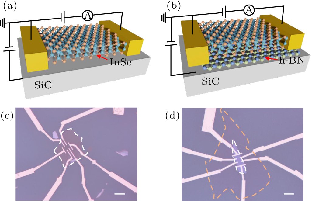
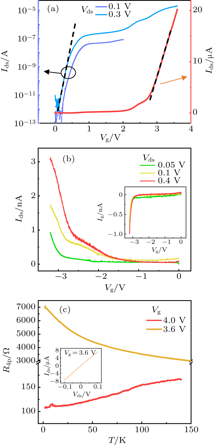
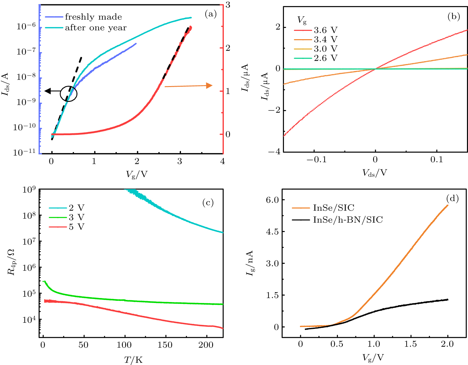
Abstract We report the electrical transport properties of InSe flakes electrostatically gated by a solid ion conductor. The large tuning capability of the solid ion conductor as gating dielectric is confirmed by the saturation gate voltage as low as ∼1 V and steep subthreshold swing (83 mV/dec). The p-type conduction behavior of InSe is obtained when negative gate voltages are biased. Chemical doping of the solid ion conductor is suppressed by inserting a buffer layer of hexagonal boron nitride (h-BN) between InSe and the solid-ion-conductor substrate. By comparing the performance of devices with and without h-BN, the capacitance of solid ion conductors is extracted to be the same as that of ∼2 nm h-BN, and the mobility of InSe on solid ion conductors is comparable to that on the SiO2 substrate. Our results show that solid ion conductors provide a facile and powerful method for electrostatic doping.
|
Received: 15 May 2020
Revised: 05 July 2020
Accepted manuscript online: 15 July 2020
|
| Fund: the National Key Research and Development Projects of China (Grant Nos. 2016YFA0202300 and 2018FYA0305800), the National Natural Science Foundation of China (Grant Nos. 61674170 and 61888102), the K. C. Wong Education Foundation, the Strategic Priority Research Program of Chinese Academy of Sciences (Grant Nos. XDB30000000 and XDB28000000), and the Youth Innovation Promotion Association of Chinese Academy of Sciences (Grant No. Y201902). |
|
Corresponding Authors:
†Corresponding author. E-mail: lhbao@iphy.ac.cn ‡Corresponding author. E-mail: hjgao@iphy.ac.cn
|
Cite this article:
Zhang Zhou(周璋), Liangmei Wu(吴良妹), Jiancui Chen(陈建翠), Jiajun Ma(马佳俊), Yuan Huang(黄元), Chengmin Shen(申承民), Lihong Bao(鲍丽宏), and Hong-Jun Gao(高鸿钧) Electrostatic gating of solid-ion-conductor on InSe flakes and InSe/h-BN heterostructures 2020 Chin. Phys. B 29 118501
|
| [1] |
Ahn C H, Bhattacharya A, Di Ventra M, Eckstein J N, Frisbie C D, Gershenson M E, Goldman A M, Inoue I H, Mannhart J, Millis A J, Morpurgo A F, Natelson D, Triscone J M 2006 Rev. Mod. Phys. 78 1185 DOI: 10.1103/RevModPhys.78.1185 |
| [2] |
|
| [3] |
Cao Y, Fatemi V, Demir A, Fang S, Tomarken S L, Luo J Y, Sanchez-Yamagishi J D, Watanabe K, Taniguchi T, Kaxiras E, Ashoori R C, Jarillo-Herrero P 2018 Nature 556 80 DOI: 10.1038/nature26154 |
| [4] |
Pei T, Bao L, Ma R, Song S, Ge B, Wu L, Zhou Z, Wang G, Yang H, Li J, Gu C, Shen C, Du S, Gao H J 2016 Adv. Electron. Mater. 2 1600292 DOI: 10.1002/aelm.201600292 |
| [5] |
Wang G C, Wu L M, Yan J H, Zhou Z, Ma R S, Yang H F, Li J J, Gu C Z, Bao L H, Du S X, Gao H J 2018 Chin. Phys. B 27 077303 DOI: 10.1088/1674-1056/27/7/077303 |
| [6] |
|
| [7] |
Yu Y, Yang F, Lu X F, Yan Y J, ChoYong H, Ma L, Niu X, Kim S, Son Y W, Feng D, Li S, Cheong S W, Chen X H, Zhang Y 2015 Nat. Nanotechnol. 10 270 DOI: 10.1038/nnano.2014.323 |
| [8] |
Braga D, Gutiérrez Lezama I, Berger H, Morpurgo A F 2012 Nano Lett. 12 5218 DOI: 10.1021/nl302389d |
| [9] |
|
| [10] |
Li E, Zhang R Z, Li H, Liu C, Li G, Wang J O, Qian T, Ding H, Zhang Y Y, Du S X, Lin X, Gao H J 2018 Chin. Phys. B 27 086804 DOI: 10.1088/1674-1056/27/8/086804 |
| [11] |
Liu H, Bao L, Zhou Z, Che B, Zhang R, Bian C, Ma R, Wu L, Yang H, Li J, Gu C, Shen C M, Du S, Gao H J 2019 Nano Lett. 19 4551 DOI: 10.1021/acs.nanolett.9b01412 |
| [12] |
Guo H, Chen H, Que Y D, Zheng Q, Zhang Y Y, Bao L H, Huang L, Wang Y L, Du S X, Gao H J 2019 Chin. Phys. B 28 056107 DOI: 10.1088/1674-1056/28/5/056107 |
| [13] |
Li L J, O’Farrell E C T, Loh K P, Eda G, Özyilmaz B, Castro Neto A H 2016 Nature 529 185 DOI: 10.1038/nature16175 |
| [14] |
|
| [15] |
Deng Y, Yu Y, Song Y, Zhang J, Wang N Z, Sun Z, Yi Y, Wu Y Z, Wu S, Zhu J, Wang J, Chen X H, Zhang Y 2018 Nature 563 94 DOI: 10.1038/s41586-018-0626-9 |
| [16] |
|
| [17] |
|
| [18] |
Lu J, Zheliuk O, Chen Q, Leermakers I, Hussey N E, Zeitler U, Ye J 2018 Proc. Natl. Acad. Sci. USA 115 3551 DOI: 10.1073/pnas.1716781115 |
| [19] |
Huang Y, Sutter E, Wu L M, Xu H, Bao L, Gao H J, Zhou X J, Sutter P 2018 ACS Appl. Mater. Interfaces 10 23198 DOI: 10.1021/acsami.8b05932 |
| [20] |
|
| [21] |
Lei B, Wang N Z, Shang C, Meng F B, Ma L K, Luo X G, Wu T, Sun Z, Wang Y, Jiang Z, Mao B H, Liu Z, Yu Y J, Zhang Y B, Chen X H 2017 Phys. Rev. B 95 020503 DOI: 10.1103/PhysRevB.95.020503 |
| [22] |
Ying T P, Wang M X, Wu X X, Zhao Z Y, Zhang Z Z, Song B Q, Li Y C, Lei B, Li Q, Yu Y, Cheng E J, An Z H, Zhang Y, Jia X Y, Yang W, Chen X H, Li S Y 2018 Phys. Rev. Lett. 121 207003 DOI: 10.1103/PhysRevLett.121.207003 |
| [23] |
|
| [24] |
Zeng J, Liu E, Fu Y, Chen Z, Pan C, Wang C, Wang M, Wang Y, Xu K, Cai S, Yan X, Wang Y, Liu X, Wang P, Liang S J, Cui Y, Hwang H Y, Yuan H, Miao F 2018 Nano Lett. 18 1410 DOI: 10.1021/acs.nanolett.7b05157 |
| [25] |
Philippi M, Gutiérrez-Lezama I, Ubrig N, Morpurgo A F 2018 Appl. Phys. Lett. 113 033502 DOI: 10.1063/1.5038407 |
| [26] |
Bandurin D A, Tyurnina A V, Yu G L, Mishchenko A, Zólyomi V, Morozov S V, Kumar R K, Gorbachev R V, Kudrynskyi Z R, Pezzini S, Kovalyuk Z D, Zeitler U, Novoselov K S, Patanè A, Eaves L, Grigorieva I V, Fal’ko V I, Geim A K, Cao Y 2017 Nat. Nanotechnol. 12 223 DOI: 10.1038/nnano.2016.242 |
| [27] |
Li L, Yu Y, Ye G J, Ge Q, Ou X, Wu H, Feng D, Chen X H, Zhang Y 2014 Nat. Nanotechnol. 9 372 DOI: 10.1038/nnano.2014.35 |
| [28] |
Wu L, Shi J, Zhou Z, Yan J, Wang A, Bian C, Ma J, Ma R, Liu H, Chen J, Huang Y, Zhou W, Bao L, Ouyang M, Pantelides S T, Gao H J 2020 Nano Res. 13 1127 DOI: 10.1007/s12274-020-2757-1 |
| [29] |
Hamer M, Tóvári E, Zhu M, Thompson M D, Mayorov A, Prance J, Lee Y, Haley R P, Kudrynskyi Z R, Patanè A, Terry D, Kovalyuk Z D, Ensslin K, Kretinin A V, Geim A, Gorbachev R 2018 Nano Lett. 18 3950 DOI: 10.1021/acs.nanolett.8b01376 |
| [30] |
Premasiri K, Radha S K, Sucharitakul S, Kumar U R, Sankar R, Chou F C, Chen Y T, Gao X P A 2018 Nano Lett. 18 4403 DOI: 10.1021/acs.nanolett.8b01462 |
| [31] |
Zeng J, Liang S J, Gao A, Wang Y, Pan C, Wu C, Liu E, Zhang L, Cao T, Liu X, Fu Y, Wang Y, Watanabe K, Taniguchi T, Lu H, Miao F 2018 Phys. Rev. B 98 125414 DOI: 10.1103/PhysRevB.98.125414 |
| [32] |
Lin C Y, Ulaganathan R K, Sankar R, Chou F C 2017 AIP Adv. 7 075314 DOI: 10.1063/1.4995589 |
| [33] |
Xue J, Sanchez-Yamagishi J, Bulmash D, Jacquod P, Deshpande A, Watanabe K, Taniguchi T, Jarillo-Herrero P, LeRoy B J 2011 Nat. Mater. 10 282 DOI: 10.1038/nmat2968 |
| [34] |
Bediako D K, Rezaee M, Yoo H, Larson D T, Zhao S Y F, Taniguchi T, Watanabe K, Brower-Thomas T L, Kaxiras E, Kim P 2018 Nature 558 425 DOI: 10.1038/s41586-018-0205-0 |
| [35] |
Sze S M, Ng K K 2006 Physics of Semiconductor Devices New York John Wiley & Sons 315
|
| [36] |
Dean C R, Young A F, Meric I, Lee C, Wang L, Sorgenfrei S, Watanabe K, Taniguchi T, Kim P, Shepard K L, Hone J 2010 Nat. Nanotechnol. 5 722 DOI: 10.1038/nnano.2010.172 |
| No Suggested Reading articles found! |
|
|
Viewed |
|
|
|
Full text
|
|
|
|
|
Abstract
|
|
|
|
|
Cited |
|
|
|
|
Altmetric
|
|
blogs
Facebook pages
Wikipedia page
Google+ users
|
Online attention
Altmetric calculates a score based on the online attention an article receives. Each coloured thread in the circle represents a different type of online attention. The number in the centre is the Altmetric score. Social media and mainstream news media are the main sources that calculate the score. Reference managers such as Mendeley are also tracked but do not contribute to the score. Older articles often score higher because they have had more time to get noticed. To account for this, Altmetric has included the context data for other articles of a similar age.
View more on Altmetrics
|
|
|