


Transient thermal analysis as measurement method for IC package structural integrity
[Hanß Alexander, Schmid Maximilian, Liu E, Elger Gordon† ]
]
]
|
|


†Corresponding author. E-mail: Gordon.Elger@thi.de
Practices of IC package reliability testing are reviewed briefly, and the application of transient thermal analysis is examined in great depth. For the design of light sources based on light emitting diode (LED) efficient and accurate reliability testing is required to realize the potential lifetimes of 105 h. Transient thermal analysis is a standard method to determine the transient thermal impedance of semiconductor devices, e.g. power electronics and LEDs. The temperature of the semiconductor junctions is assessed by time-resolved measurement of their forward voltage ( Vf). The thermal path in the IC package is resolved by the transient technique in the time domain. This enables analyzing the structural integrity of the semiconductor package. However, to evaluate thermal resistance, one must also measure the dissipated energy of the device (i.e., the thermal load) and the k-factor. This is time consuming, and measurement errors reduce the accuracy. To overcome these limitations, an innovative approach, the relative thermal resistance method, was developed to reduce the measurement effort, increase accuracy and enable automatic data evaluation. This new way of evaluating data simplifies the thermal transient analysis by eliminating measurement of the k-factor and thermal load, i.e. measurement of the lumen flux for LEDs, by normalizing the transient Vf data. This is especially advantageous for reliability testing where changes in the thermal path, like cracks and delaminations, can be determined without measuring the k-factor and thermal load. Different failure modes can be separated in the time domain. The sensitivity of the method is demonstrated by its application to high-power white InGaN LEDs. For detailed analysis and identification of the failure mode of the LED packages, the transient signals are simulated by time-resolved finite element (FE) simulations. Using the new approach, the transient thermal analysis is enhanced to a powerful tool for reliability investigation of semiconductor packages in accelerated lifetime tests and for inline inspection. This enables automatic data analysis of the transient thermal data required for processing a large amount of data in production and reliability testing. Based on the method, the integrity of LED packages can be tested by inline, outgoing inspection and the lifetime prediction of the products is improved.
The efficiency of light emitting diodes has been continually increased during the last decade, and efficacies exceeding 300 lm/W were reported recently.[1– 3] Due to this development, also less waste heat is generated in the device and the question might arise whether thermal management will lose importance? Unfortunately — or maybe fortunately for thermal engineers — that question will remain rhetorical for long time. With the ongoing trend of miniaturization in electronics and the need for cost effective but reliable products, heat management remains one of the crucial engineering design limitations. By basic laws of nature such as the Arrhenius equation the operating temperature is always connected to the lifetime and reliability of semiconductor devices. Large changes of the operating temperature due to on– off conditions also cause thermo-mechanical stress and mechanically induced failures in electronic modules, e.g., cracks and delamination.
Reliability and long service life will determine the economic and ecological success of LED illumination systems. LED systems can, in general, reach a very long lifetime of up to 105 h when appropriately designed. Business models are based on the failure-free operation of light sources for the defined long lifetime. Junction temperature and drive current are the parameters that determine lumen degradation and lifetime of the LED. In addition to the slow lumen degradation, catastrophic failures of the LED can also occur. For eliminating these failures, not only die and package design, but also process and material control in manufacturing, is important. Finally the environmental conditions during operation, like humidity, corrosive atmosphere, and thermo-mechanical stress, are fundamental for the targeted lifetime of the LED systems.
Many failures are driven by the junction temperature TJ of an LED. Thermal management is therefore essential for the design of cost competitive and reliable LED systems. Experimental and simulation methods for heat management are important. Many different thermal analysis tools and techniques are available with their specific advantages for a given application under specified boundary conditions. Thermal assessment requires a combination of different measurement techniques, analytical and numerical analysis to support and validate their conclusions.
Transient thermal analysis, i.e., the time-resolved measuring of TJ by the forward voltage Vf, is a powerful approach to measure the junction temperature of the LEDs in a system and the thermal resistance Rth of the LED module.[4– 8] The heat flow passing through an LED module can be resolved. Transient thermal analysis has become a common method and it is standardized in the MIL-STD-750F (3100 Series).[9] Also the Solid State Technology Association (JEDEC) has published in their JESD51 series valuable standards and thermal characterization test methods.[10] They are applicable to a wide variety of semiconductor packages under different mountings and usage conditions and underpin the thermal specifications of the manufacturer.
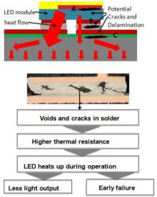
Transient thermal analysis can also be applied for reliability testing. After switching the heat load the forward voltage Vf(t) is measured time-resolved, and the thermal path from the die through the LED package to the heat sink can be accessed. The location of failures can be identified. For example, it is possible to distinguish between failures such as delamination of the LED die or cracking of the solder connecting the LED package to the printed circuit board (PCB). In Fig. 1 typical failures as solder joint cracking or die delamination are depicted. Those failures disrupt the thermal path and can be observed by the transient thermal analysis. The failures do influence the reliability of the LED in several ways: The junction temperature will increase leading to a faster degradation, local overheating can cause a catastrophical failure or an electric contact, e.g. solder joint, will crack and fail as “ open contact” .
 | Fig. 1. Effects on the reliability of an LED module by failures like A: delamination of die bond, B: crack in solder joint, C: delamination of dielectric layer of Al-IMS. The cracks and delamination block the thermal path and the temperature increases. The changes in the heat flow path can be observed by transient thermal analysis. For a more detailed description of an LED package, see Fig. 2. |
However, the transient thermal measurements are often considered to be complicated and time consuming. The thermal load and the proportional factor between temperature and forward voltage have to be measured. Today the structural function is the predominant approach to analyze the transient temperature data. It plots the cumulative thermal capacity Cth dependent upon the cumulative thermal resistance Rth alongside the heat flow path (one-dimensional approximation). On one hand, it is very useful because it lets the user directly access the thermal resistance but on the other hand, it is susceptible to measurement artifacts like the response of the temperature regulation of the thermal stage, the dead time of the transient tester and noise and artifacts on the time curve. However, most of these artifacts are visible on the time-derived curve and can be avoided or eliminated before further data processing.
The thermal boundary conditions influence the measurement and the LEDs under test have to be very reproducibly connected to the heat sink of the measurement equipment to avoid mistakes. The potential for failures in the measurement set-up and data evaluation often require a thermal expert for this analysis. Standardization and documentation help counteract the potential for failure. However automatic customized data evaluation is still the bottleneck in many companies for applying transient thermal analysis on a larger production scale. Transient thermal analysis is a method for advanced test labs but not widespread in high volume testing in production or in-line testing.
As a simplification, the measurement of the relative thermal resistance was introduced[11] in 2011. It was demonstrated that the transient thermal analysis can be applied in production to inspect the solder joints of high power LED modules. The normalized time-derived Vf(t) curves of the samples under test were compared with those of known good reference samples. The sensitivity was benchmarked to acoustic microscopy (CSAM) inspection. Inline Rth inspection was introduced based on the normalization method.[12] Later, the method was improved and extended to investigate the reliability of the ceramic LED packages on printed circuit boards (PCB) during reliability tests.[13] Instead of the normal time derivation logarithmic time derivation was used and the method of normalization was improved. The predominant PCB for LED modules is insulated metal substrates (IMS) using aluminum as metal core (Al-IMS). A huge variety of Al-IMS exists, with optimized thermal conductivity and thickness of the dielectric layer and a large variation in cost/m2. Immediately, the question arises whether money is well invested in expensive material for heat management. This is extremely relevant because the reliability aspect is often more important than the thermal aspect and much more difficult to assess. The new method, i.e., transient thermal analysis of the relative thermal resistance, was developed to facilitate and speed up the reliability assessment of LEDs. In many test laboratories the solder joint failure in LED assemblies is still tested by a simple light-on test. It has been demonstrated that the new method is far more sensitive than the still dominant light-on test.[14] In the present paper, the application of the new method is reviewed.
For data evaluation, transient finite element (FE) simulation is an important tool to determine the physical parameters of an LED module. Due to the progress in computational resources and FE simulation tools, transient simulation of real trree-dimensional (3D) models can be performed without extensive model preparation and long computation time. The real 3D heat flow is assessed, which is an important advantage compared to one-dimensional (1D) equivalent network simulations. The steady state and transient measurement data can be simulated and changes in the experimental transient data can be analyzed by the simulation. Based on a validated transient FE model, the root cause of the failure can be identified.
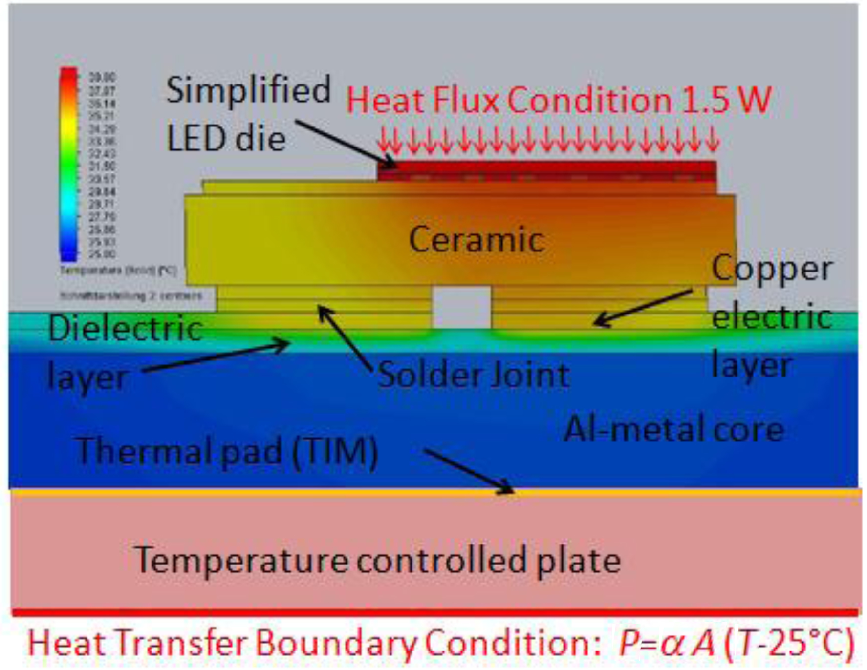
When an LED is operated, only a part of the electric input power is converted into light. The efficiency of the LED is called wall plug efficiency (WPE). Under realistic operating conditions nowadays, WPE is between 20%– 40%. The remaining power, i.e., the thermal load Pth, is dissipated as heat. The thermal load is calculated from the WPE and the electric input power Pel:

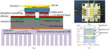
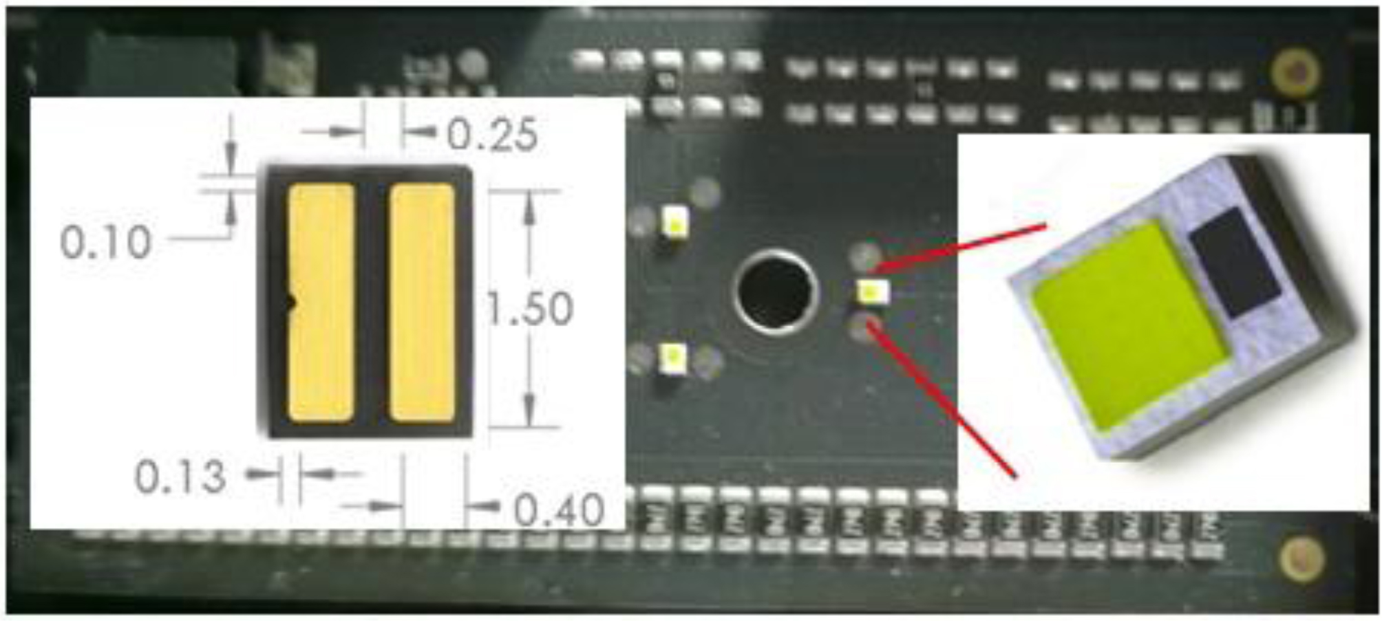
The thermal load has to be transferred by heat conduction from the LED die through the package and the printed circuit board (PCB) to the heat sink. The theory of heat conduction is governed by Fourier’ s law and described in text books such as Ref. [15]. The heat flow is linearly dependent upon the temperature gradient between the junction and the ambience. In the following, TJ denotes the temperature of the junction and TA the ambient temperature. In Fig. 2 the scheme of an LED ceramic package on Al-IMS is depicted. The small semiconductor die is bonded on the ceramic heat spreader. The ceramic heat spreader is soldered on the electric layer of the Al-IMS. The dielectric layer of the IMS is located between the electric layer and the Al-core. The Al-IMS is connected with a thermal interface material to the heat sink, which dissipates the thermal energy to the ambient air.
 | Fig. 2. Schematic drawing of a ceramic LED package on Al-IMS (a), test module (b), and footprint of LED package (c). |
The thermal resistance Rth_real of an LED module is defined as the temperature increase divided by the thermal load Pth, which is conducted through the module and causes the temperature increase. The thermal resistance from junction to the ambience of a module, as depicted in Fig. 2, is therefore calculated by

If the Al-IMS is mounted on a temperature-controlled plate instead of the heat sink, TA has to be replaced by the temperature of the temperature-controlled plate TP. The thermal resistance obtained by Eq. (2) of the LED package on the Al-IMS includes the thermal resistance of the TIM between temperature-controlled plate and LED module. Care has to be taken if in real systems the temperature of the temperature-controlled plate is not uniform. The temperature needs to be measured at the center location under the LED module. Also the expression “ case temperature” Tcase is used, which denotes the maximum temperature below the LED module. Actually, Tcase is located above the TIM and larger than TP of the temperature-controlled plate.
If the heat transfer is uniform throughout the surface area A of a solid material the thermal resistance can be calculated by Fourier’ s law:

where L is the thickness of the solid, and λ is the thermal conductivity. This formula is always very handy to estimate the thermal resistance before starting any FE simulation.
The index “ real” for the thermal resistance of an LED was introduced by JESD51-51 and is used to a peculiar history of LED thermal resistance measurements. As long as the WPE is very small, the energy emitted by light is not considered for calculation of the thermal load and the thermal resistance Rth. Directly, the electrical power is used as thermal load to calculate the thermal resistance. This Rth is today called “ electrical thermal resistance” and should be indicated by the index “ el, ” i.e. Rth_el:

With the increase of efficiency and WPEs above 20%, one has to distinguish carefully between Rth_real and Rth_el. In many old data sheets the symbol Rth designates the “ electrical-thermal” resistance Rth_el. Unfortunately, also today some data sheets use solely Rth and it remains unclear what is really meant. The Rth_el, which is for thermal engineers a somehow strange definition, is actually quite useful to calculate the temperature increase within an LED package without bothering for the real thermal load of the LED. However, it is temperature-dependent due to the dependence of the LED efficiency upon the temperature, i.e. hot– cold factor. For the calculation of the thermal resistance of an LED system, obviously the Rth_real and the real thermal load has to be used. Otherwise the system would be designed to dissipate more heat than the real system will produce. The denotation Rth_el and Rth_real is a nuisance, but for the present it is necessary to avoid ambiguities. It is therefore applied in this paper. In the following the expression Rth is solely used when it does not matter whether Rth_el or Rth_real is referred to.
To determine the Rth, the temperature gradient within an LED system has to be measured. The forward voltage Vf of the junction of a semiconductor is a valuable temperature probe due to its temperature dependence. The nonlinear dependence can be derived from semiconductor theory by the Shockley equation.[16, 17] Nevertheless, in an adequate small temperature range (typically within 50 ° C) it can be linearly approximated for a defined drive current:

The linear factor k, called the k-factor or sensitivity of Vf(t) to temperature T, is in the range of 2 mV. The constant Ucon is due to contact resistance of the probing system and the inner serial resistance of the LED. The k-factor depends upon the energy bands and the effective electronic state densities of the junction and, therefore, also upon internal and packaging-induced stress in the junction. The k-factor may vary for a single LED from wafer to wafer in a batch between 1 mV and 3 mV. After determination of the k-factor for a specific drive current, the forward voltage can be used to calculate the temperature change in the LED junction when a specific current is applied. However, the k-factor can change during reliability testing depending upon the device and epitaxial design of modern LEDs.[18] The same holds for the LED efficiency. The lumen flux as well as the thermal load change during accelerated lifetime testing of the LEDs. Therefore, to obtain an accurate thermal resistance Rth_real the k-factor and the lumen flux need to be measured again after every interval of accelerated lifetime testing. This requires a significant amount of experimental effort and is unsuitable for large volume reliability testing or inline inspection.
As discussed in the introduction, transient thermal analysis is a common method to measure the thermal resistance of microelectronic packages that contain active semiconductor devices. The thermal response of a system like an LED package on a printed circuit board is measured time-resolved, after switching a heat load as shown in Fig. 3.
 | Fig. 3. The heat load is switched by the drive current of the LED. During heating up under high drive current Vf decreases from the initial large value. Due to switching from a large drive current to a small sensing current Vf is initially reduced because the required Vf at lower current is smaller (V(I) characteristic curve) and rises afterward while the junction cools down. |
Initially a constant heat flux by a large drive current (Idrive) is applied until thermal equilibrium is reached in the package. The thermal equilibrium is then changed by switching off the heat flux. The forward voltage Vf(t) is measured, time-resolved, by applying a small sensing current Isense while the system transfers into its new thermal equilibrium. The temperature T(t) is obtained from Vf(t) by Eq. (5). For accurate absolute temperature measurements the contact resistance Ucon in Eq. (5) needs to be small or very reproducible. Transient testing determines the difference Δ Vf = Vf (junction hot) − Vf (junction cold) and is independent of Ucon, and by that, independent of the contact resistance. However, one needs to measure the Vf in hot condition, i.e., heat flux switched on for sufficiently long time that the thermal equilibrium is reached, and Vf in cold condition (heat flux switched off for sufficiently long time that the thermal equilibrium is reached) for the same drive current Isense. After switching off the drive current from Idrive to Isense, a short delay time, i.e. dead time, is required until the system has stabilized after current switching before accurate Vf data can be obtained. The dead time is discussed in more detail below in Section 3. The same holds when measuring heating up of the device besides that under high current conditions noise is increased. In addition, while heating up, the thermal load changes due to a change of WPE, dependent upon temperature. Cooling down measurements are therefore preferred. However, for in-line measurements, heating up data are also useful and utilized.
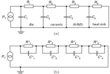
As indicated in Fig. 2, the thermal capacities in microelectronic assemblies are usually ordered following the thermal path from TJ to TA, i.e. starting from the very small heat capacity of the LED die and ending with the large capacity of the heat sink: die (very small), ceramic heat spreader (small), Al-IMS core (medium), heat sink (large), and ambient air (infinite). Intermediate thin layers and contacts like the interconnection between die and ceramic, the dielectric layer of the IMS and the thermal interface between Al-IMS core and heat sink are considered as thermal resistances. The thermal masses of the intermediate layers are small as long as they are very thin compared to the thick layers of the main thermal capacities. One can draw a simplified equivalent network for this heat transfer problem, as in Fig. 4(a).[19, 20] Limitations of this simplified 4-node network are immediately visible. The electric layer and the solder joint are not considered separately. They are included in the ceramic heat spreader node in this simplified 4-node network. This is acceptable as long as the thermal masses are small. Anyway, the system should be described using more nodes. However, instead of discussing the number of nodes required for modeling, the basic solution of an n-node equivalent network will be clarified. In the transient analysis for the cooling-down measurement, the system is represented by a step function Pth(t) = Pth· (1 − ε (t)) with ε (t) being the unit step function which switches at t = 0 from zero to one. The temperature of the Cauer network is solved by transforming it first into an unphysical Foster network by partial fraction decomposition, as depicted in Fig. 4(b). The general approach that is still used today was published 1959.[21] The solution of an n-node Foster network can be straightforwardly calculated analytically:

Pth is the dissipated thermal load in the LED and 

where 

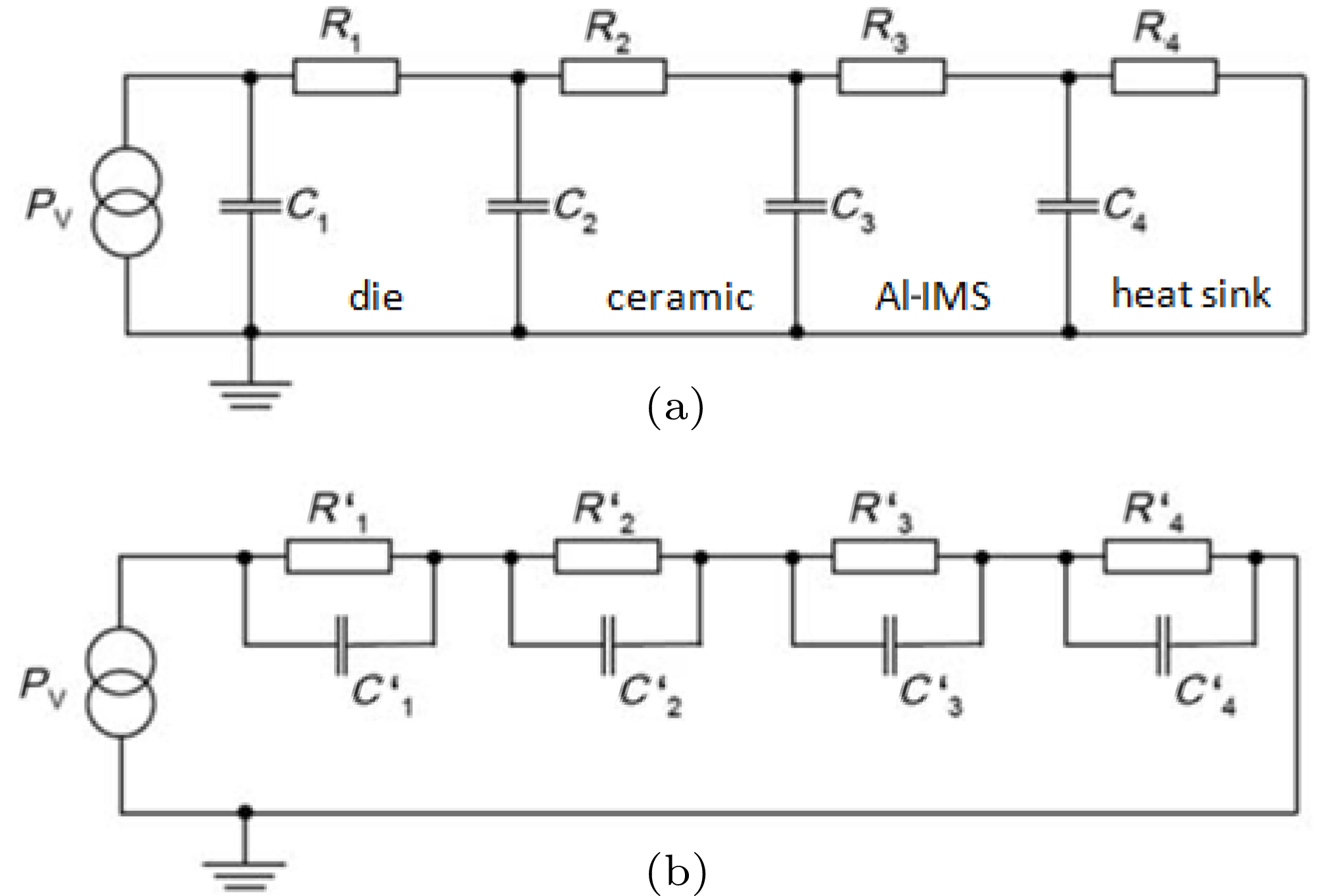 | Fig. 4. Simplified equivalent network of the ceramic LED package of Al-IMS. In panel (a) the physical Cauer Network is represented. The physical thermal masses are “ charged” with heat in reference to the ambient temperature, which is equivalent with the ground. Four main capacities are approximated: C1 = Cdie, C2 = Cceramic, C3 = CAl-core, C4 = Cheat sink. The thermal masses of the electric layer and the solder joint are included in C2. The thermal resistances are approximated: R1 contains the thermal resistance of the die and the interconnect of the die to the ceramic (R1 = Rdie + Rinterconnect), R2 contains the thermal resistance of the ceramic (small), the solder joint (medium) and the electric copper layer (small) and the dielectric layer of the IMS (large), R3 contains the thermal resistance of the Al-core (small) of the IMS and the TIM (large) to the heat sink, R4 contains the thermal resistance of the heat sink and the thermal resistance of the heat sink to the ambient air temperature. (b) The physical Cauer network can be transformed by partial fraction decomposition into the Foster network. |
By dividing Eq. (6) through the thermal load Pth the transient thermal impedance Zth(t) is obtained

Using an n-node model the
The numerical calculation of the thermal system based on Cauer network representation is one-dimensional. When solving the network, the effect of heat spreading will be included in the capacities Ci and resistances Ri of the network. When structural changes in the module occur during reliability testing, e.g., the heat spreading changes due to cracks or delamination, the parameters of the model, i.e., the Ri and Ci, will change. Note that due to a different heat path, heat distribution in the physical model and the capacities of the model change because a different amount of thermal energy is stored in the module.
As discussed in the earlier sections, for determination of the thermal resistance Rth_real in addition to the transient Vf(t) curve, the k-factor and the thermal load have to be measured. For reliability testing, the focus of interest is structural integrity. Only relative changes in the heat path have to be investigated. In the following, the concept of the relative thermal resistance measurement for reliability testing will be developed, which avoids measurement of the k-factor and thermal load. Actually, the concept is in general rather straightforward, and it is nothing more than a normalization of the transient response in the time domain.
Basically the impulse response of the thermal network is time-derived from the measured Vf(t) curve. Due to the exponential dependence upon time, the information is more pronounced on the logarithmic time scale. Therefore, the first one substitutes ν = ln(t) and afterward calculates the logarithmic time derivation:

In the following equation (5) is inserted in Eq. (9)

Equation (10) is the starting point for further data processing. First of all it is readily apparent that the k-factor and thermal load are solely linear scaling factors. As usual, to eliminate linear factors one applies the logarithm and defines B(ν ):

In the logarithmic representation B(ν ), the proportional factor 1/(k · Pth) is transformed into a constant axis offset. Changes in the thermal load or the k-factor move B(ν ) perpendicular to the ν axis (logarithmic t axis) but do not influence the shape of the curve. In contrast, changes in the thermal resistance change the shape of the curve. Assuming, for example, that no changes in Rth_real occur during reliability testing, but the k-factor or thermal load does change, the shape of the curves remains identical but the curves are moved perpendicular to the ν axis (t axis). By an appropriate shift, the curves will fully overlap. The procedure of normalization is demonstrated in Fig. 5 using real measurement data. For measurement, a commercial T3Ster with software from MICRED is used. Vf(t) is measured for different drive currents (800 mA, 700 mA, 600 mA) for a ceramic LED package as depicted in Fig. 2, and the normalized transient temperature data are obtained by dividing through Pel (left top). The structural function is calculated (left bottom). Due to the power dependence of efficiency, the Rth_el of the 800-mA curve is larger, i.e., the tear-off edge is at higher Rth values. The logarithmic time-derived curves are depicted as calculated from the Vf(t) curve, i.e., the curves are not divided by the electrical load Pel (right top). B(ν ) curves are plotted (center) and afterward B(ν ) is normalized, i.e., all curves are moved on top of each other. It is clearly visible, as it should be, that the thermal path for all three curves is the same. To normalize the curves it is only necessary to divide all B(ν ) values of the curves through the B(ν n) at the normalization point, i.e., the central point of the normalization interval.
 | Fig. 5. Example of normalization procedure. Transient thermal curves are measured using different drive currents. 600 mA/700 mA/800 mA. The Rth_el grows with increased drive current because the efficiency of the junction decreases slightly. The time-derived curves are moved up and the peaks increase due to the higher thermal load. Note that the time derived curves are not divided through the electrical load. In contrast, the Rth_real, i.e., the thermal path, remains constant. This becomes visible after taking the logarithm of the time-derived curve and performing normalization. The simplest way of normalization is to divide every measured value of a measurement curve through the value at the center of the normalization area. To reduce potential errors due to noise the red and black curves are fitted on the blue curve by a least squares fit of a constant axis offset. It is readily apparent that all three curves precisely overlap; therefore the thermal path and Rth_real are identical. |
For noise reduction, the correct value for the shift can be obtained by a least squares fit of the linear axis offset, that is, moving the curves on the top of each other and minimizing the residuals in a chosen time interval, as indicated in Fig. 5 (bottom right). The value of the shift ashift is fitted by minimizing the R(ν n), i.e., the sum of the squared residuals within the fit interval [ν n − ν 0, ν n + ν 0] as described in the following Eq. (12):

It is important to remember that the relative position in a logarithmic plot is necessary only when an axis offset from the y axis is to be calculated. For the integrity of the thermal path, the shift is not relevant. However, the shift is relevant in obtaining the real thermal resistance from the relative thermal resistance. One needs to use a known good reference sample for which thermal load and k-factor have been determined. By calculating the ashift of the reference sample Rth_real can be calculated.
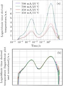
As a second example, a 1-W high-power LED is measured under different conditions, i.e. temperatures 25 ° C and 55 ° C and drive currents 350 mA and 700 mA, in Fig 6. The measured B(ν ) curves have different amplitudes due to differences in thermal load. The dissipated energy at higher temperature is reduced due to the reduction of Vf with increased temperature. At higher temperature the efficiency of the LED drops and the Rth_el increases. The derived temperature curves depicted are not normalized, i.e., it is the derivation of the temperature rise and not of the normalized temperature. Therefore the Vf drop produces a much stronger effect than the WPE drop does. However, after normalization of the logarithmic representation, the curves overlap except for some measurement noise.
 | Fig. 6. 1-W high-power LED measured at different temperatures (25 ° C and 55 ° C) and different drive currents. The time derived curves have different amplitudes due to the different thermal loads. (a) One can notice that at 55 ° C (red) with 350 mA drive current, less heat is generated than at 25 ° C with 350 mA due to the drop of Vf at higher temperature 55 ° C (red). At 700 mA the amplitude of the signal is much larger. The two curves measured at 700 mA at the same temperature of 25 ° C overlap fully (green and blue curves). (b) After normalization, all curves overlap perfectly because the heat flow in the sample is the same. At early times and very long times, the influence of noise is visible. This unit a.u. is the abbreviation for arbitrary unit. |
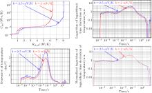
A third example is depicted in Fig. 7. A ceramic LED package is measured twice. For the first measurement, a k-factor of k = 2 mV/K and for the second k = 2.5 mV/K is used, i.e., simulating the use of a wrong k-factor. The structure function of the measurement with k = 2.5 mV/K presents a larger Rth_el than that of the measurement with k = 2 mV/K, due to the different scaling. The calculated temperature rise is smaller, and with it, the logarithmic time derivation for the larger k-factor. When the logarithmic time derivation is plotted on a logarithmic axis, it can be found that only the curves are shifted, and the heat flow through the sample remains precisely the same as it has to be. By normalization, the curves are moved on top of each other.
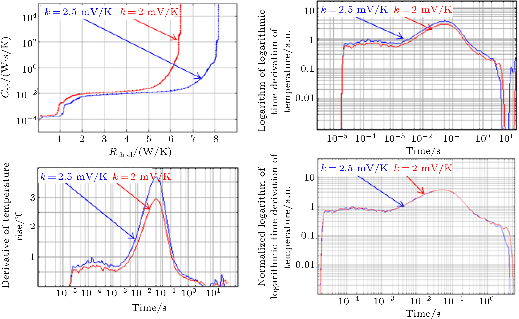 | Fig. 7. Normalization of wrong k-factor: The same ceramic LED module is measured with a MICRED T3Ster but different k-factors are used, i.e. the k-factor of 2.5, simulating a measurement error of the k-factor. It is readily apparent that the influence of the k-factor can be eliminated. |
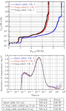
An example of the importance of evaluating data in the time domain is depicted in Fig. 8. Here the electrical load is influenced by the length of the cable between the current source and the LED module. A wrong thermal load is calculated by the measurement equipment because some of the electrical energy is dissipated in the cable. In the example, the real thermal signal does not change because the same thermal load is dissipated in the LED due to equal drive current. The structural function depends sensitively upon the total electrical load. However the logarithmic time-derived curve does not change, because the same amount of energy is dissipated in the LED module causing the same Vf(t) signal. The example is similar with using a wrong k-factor and underlines the importance of analyzing the data in the time domain.
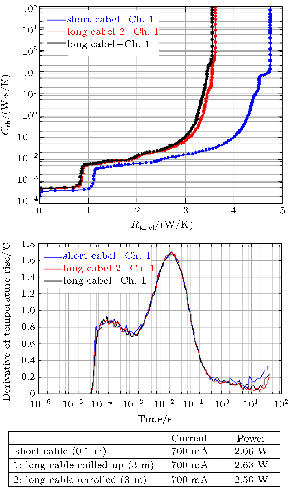 | Fig. 8. Transient temperature measurement of a ceramic LED package using an MICRED T3Ster. The cable length of the drive source to the LED is varied in an extreme way (short = 10 cm, long = 2 m) resulting in different thermal loads for the same drive current. The electric load in the cables is not subtracted, i.e., the software assumes that the full electrical load is dissipated in the LED and calculates different Rth_el structural functions, i.e., a smaller Rth_el for the long cable. However, the time-derived curves are identical, as the same amount of thermal load is dissipated in the LED. |
In a real reliability experiment, dVf(ν )/dν also varies due to changes in the thermal path, and a fit for normalization over the full ν axis would result in a flawed normalization. Therefore, solely for a selected time window, the curve measured after the reliability testing is fitted on the initial curve (0-hour curve) measured before testing. As long as the thermal path within the normalization window has not changed during the reliability, test, a residual free fit is obtained for this time interval, i.e., pure noise as residuum. However, if the thermal path changed in the time range of the normalization window, a residuum remains. This residuum indicates a real failure within the time domain of the time window. Obviously, the proper selection of the normalization window is application-dependent. It should be located in a time range where no failures are expected. However, if, in rare cases, a failure in the time window of normalization occurs, it will be identified by the residuum of the least squares fit and the sample will be identified as a “ failure in normalization time range.”
The transient thermal measurements were made using a T3Ster equipment from MICRED (Now Mentor Graphics) on one side and equipment we built in-house on the other side. The software for the relative Rth was developed in a cooperative project between Philips GmbH and Technische Hochschule Ingolstadt. The device under test (DUT) is mounted on the temperature-controlled heat sink. The heat sink is maintained at a temperature of 25 ° C and controlled by a Keithley temperature controller. Initially, a junction-to-case thermal equilibrium is ensured by applying a drive current (Idrive) for a sufficiently long duration; then the Idrive is switched off and a small sense current (Isense) is applied. When the system shifts to its new thermal equilibrium, the cooling down of the junction is measured. From the transient time curves, the duration of cooling down can be taken for how long the heating current Idrive needs to be applied to load the thermal capacities. The same time has to be measured applying Isense to resolve the thermal path downstream to the respective capacity. One approach to determine the required measurement time is to modify the thermal interface between the heat sink and the module, i.e., apply the dual thermal interface method.[10, 27] The time value at which the curve with the best possible thermal interface and one with bad thermal interface separate is approximately the appropriate time duration for Idrive and Isense when the thermal path upstream the varied thermal interface are to be investigated. One can stepwise shorten the heat-up and cool down time afterward and observe at what setting, and at which time, values change in the logarithmic time-derived curve. The shortest time for which the deviation of the time curves is still within the signal-to-noise range of the curve with long heating and cooling times is still acceptable. As an example, if the focus is within the LED package, the measurement times can be reduced to 0.5 s for the LED package investigated in Fig. 8.
For most reliability investigations performed in this paper, the k-factor and thermal load were not measured. For some samples, i.e. known good reference samples, the k-factor and lumen flux were measured to calculate Rth_real. Initially, for sensitivity investigation, the lumen flux and k-factor of some LED batches were measured for the LEDs at 0 hour and at the end of the test.
In this section, limitations and some typical measurement artifacts of the transient thermal analysis are summarized to raise awareness for avoiding measurement and analysis errors.
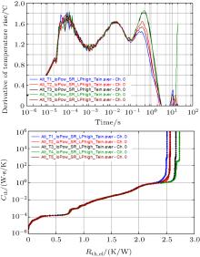
First of all, one has to be aware that when extracting the overall Rth_real or Rth_el junction-to-heat sink, the TIM is included in the measurement. For the valuation of comparable measurements it is crucial to always establish the same TIM between the LED module and the temperature controlled plate. Figure 9 shows several measurements under identical test conditions with the same set-up and LED package but different TIMs. The high variance in the last peak illustrates the big influence of the TIM on the total value of Rth_el. In the logarithmic time-derived curves it can be clearly seen that as long as the interest is the package, a measurement time of 0.1 s is sufficient to resolve the thermal path in the package. For detection of the thermal resistance of the module, the dual interface measurement method requires measuring the module with two different interfaces. The separation point indicates the Rth of the module. However the separation point still includes the best TIM of choice, i.e., the TIM influences the measurement results, and the applicability of the method depends on the package.
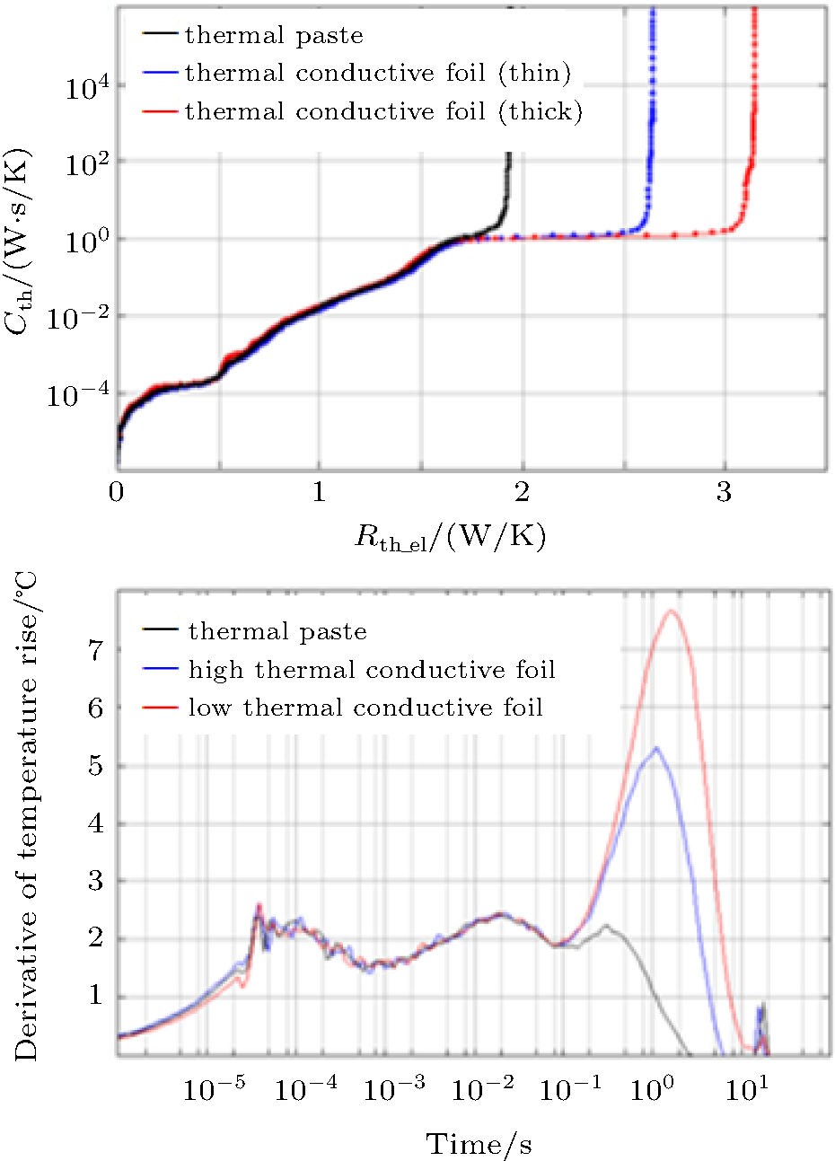 | Fig. 9. Under identical test conditions with the same set-up and device under test (DUT), three different TIMs were used. The black line displays the test with a half-liquid heat transfer paste as TIM, the red line stands for the measurements with a plastic foil TIM with a low thermal conductivity, and the blue line displays a TIM in the form of a pad with high thermal conductivity and a thickness of 0.5 mm. |
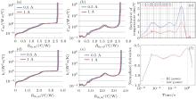
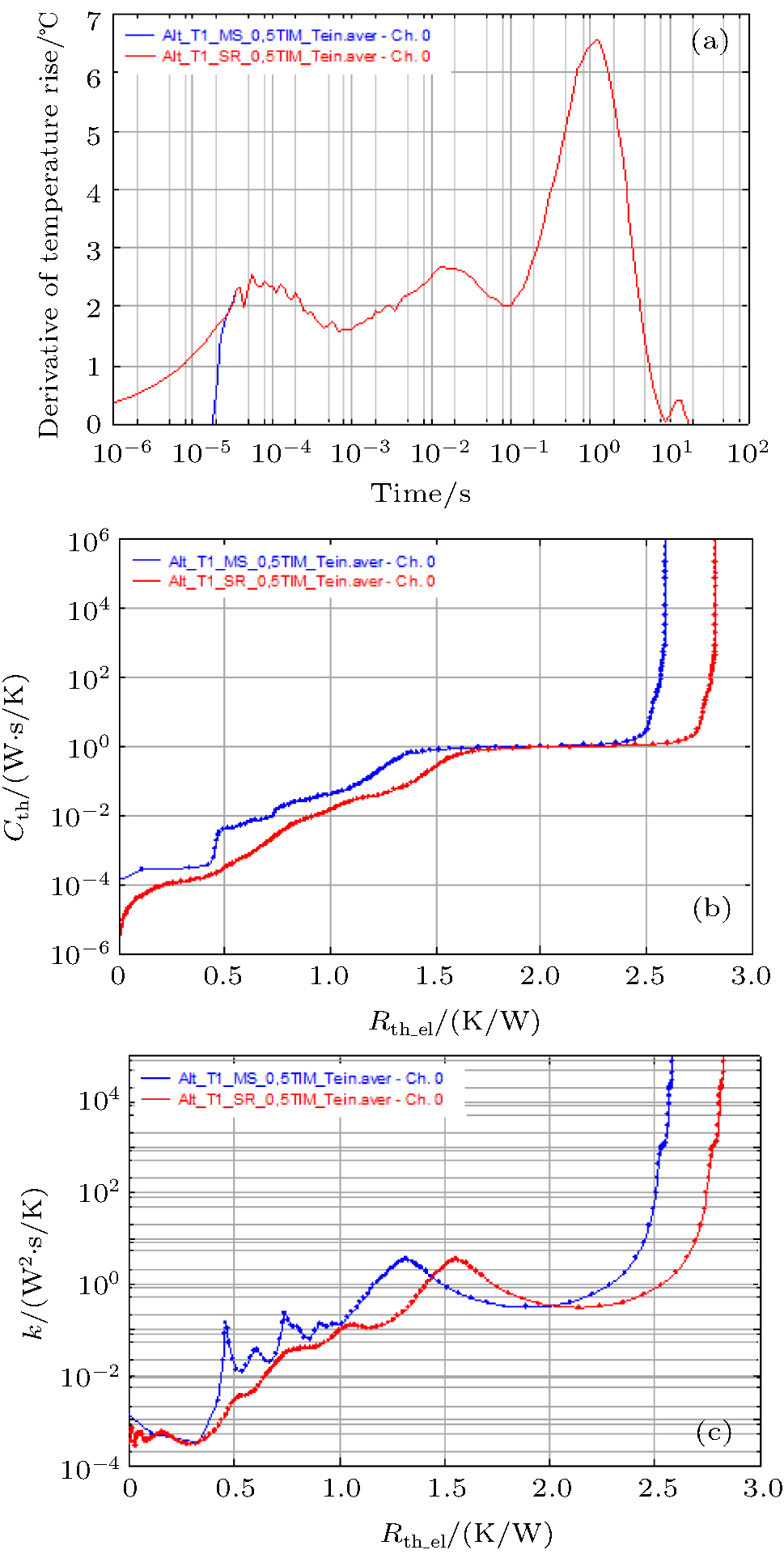
To avoid the reference measurement, a defined good thermal interface is often used, and the tear-off edge of the structural function is used for identifying the Rth of the package. The reproducibility of thermal interface materials is however limited and depends on the kind of interface material used. For demonstration, measurements performed on a LUXEON Altilon test package are depicted in Fig. 10. Deviations of ± 0.1 K/W are observed.
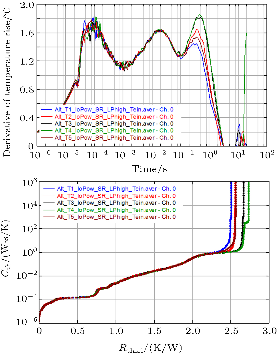 | Fig. 10. Reproducibility of the thermal interface material between module and heat sink. Thermal grease was applied between heat sink and LED module (LUXEON Altilon test package, 1-A drive current at 12 V). The module was taken off and mounted by springs (same mounting force) on the heat sink several times and measured. A significant deviation of 0.1 W/K is visible. |
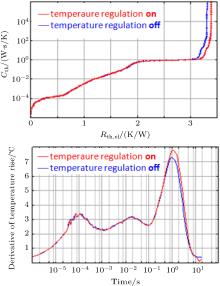
Another artifact is included and visible in Fig. 10: A short step is observed at the tear-off edge of the structural function. This is an effect of the active temperature control of the heat sink. The temperature regulation has a specific response time. The time range of the transient analysis expands from 10− 6 s to 10 s. Therefore the response of the temperature regulation is within the range of the analysis. In Fig. 11 the effect of the temperature regulation is shown. Structural functions are measured with temperature control switched “ on” and switched “ off.” The best way to suppress the effect is to use a heat sink with large thermal mass and a temperature control with a slow response time. This ensures that the response time of the temperature control is far outside the response time of the LED module.
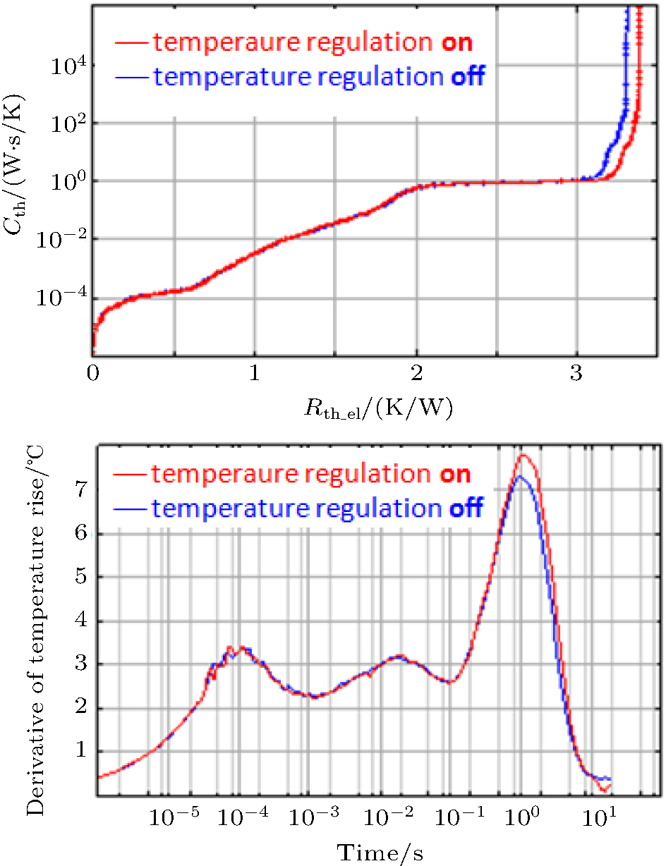 | Fig. 11. Effect of temperature regulation. The response time of the temperature regulation creates an underlying baseline in the time domain, which influences the time response and the structural function. |
An important limitation of any transient data recording equipment is the experimental dead time, i.e., the very early data of the transient cannot be measured. This is caused by the electrical response of the device and the measurement equipment due to the switching of the drive current, i.e. the diode itself and the parasitic capacity and inductance of the electrical interconnection. In Ref. [28] the different effects of the electrical responses of different semiconductor devices are summarized. The dead time of commercially available thermal testers is in the range of 10 μ s– 20 μ s. In conclusion, the contribution of the Cauer network nodes with very small capacities to the thermal resistance cannot be measured, i.e. the resistance of very thin dies. It was shown earlier[29] that the influence is significant for low Rth LED modules, and this phenomenon recently got broader attention.[30] Measurements using a lab-built transient tester reach a dead time of 6 μ s.[31] The early data have to be extrapolated. The first approach has been to cut off the early time data (minimum seek feature in the T3Ster software). This creates a discontinuity in the time domain and a distinct distortion in the structural function. The second, better approach is the “ square root feature, ” which is also mentioned in the JESD51-14 standard. The early data are extrapolated by a square root function which is the theoretical description for a junction-up diode in which the heat flow is conducted through a sufficient thick bulk layer. The square root dependence is fitted on the earliest data that are not corrupted by the electrical response of the measurement equipment and DUT. The systematic errors caused by time– zero time extrapolation are shown in Fig. 12. A difference of 0.3 W/K is obtained for the example LED module, which is roughly 25% of its value specified in the data sheet (1.2 K/W). With the “ minimum seek” feature, Rth values are calculated lower because the early data are simply cut rather than extrapolated. Obviously, the square root correction is a better approximation, but for modern thin film LEDs, it is not a suitable approach, especially for white LEDs with phosphor-containing material attached to the die. At present, one cannot conclude from LED suppliers’ data sheets how the Rth is determined. Even when LED suppliers follow the recommendations of the MICRED influenced JESD51-14 standard, different results are obtained depending upon the time interval over which the square root is extrapolated.
 | Fig. 12. Influence of the dead time extrapolation. (a) Logarithmic time derivation of a transient Vf(t) measurement of the LUXEON Altilon test package processed by “ minimum seek 20 μ s” (blue line) and “ square root 20 μ s– 40 μ s (red line).” (b) Influence of the dead time extrapolation on the structural function. (c) Influence on the derivative of the structural function (first derivation of the structural function dC/dR). |
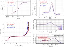
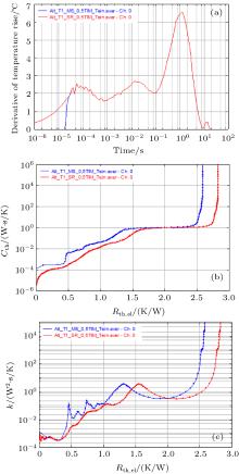
At early times, the signal to noise (S/N) in the transient Vf(t) data is large, especially for the calculated time derivation of Vf(t). In the time domain, the noise is visible and the need for better S/N in the μ s time range becomes obvious when evaluating the influence of the noise on the structural function. When just looking at the Vf(t), it might not be as evident. However, the impulse response of the system represents the system, i.e., the time derivation of Vf(t). One must use filtering algorithms that have low impact on the time response, i.e., peak position and peak shape. An example of how noise and arbitrary disruptions impact the structural function is depicted in Fig. 13. A low Rth_real, high-power LED module is measured at 1-A and at 0.5-A drive currents. The heat flow through the module is the same, and the same Rth_real should be obtained. The Rth_el is slightly higher for 1 A because the WPE drops for high drive currents. On the normalized logarithmic time derivation, one can immediately recognize that the heat flow is the same. However, due to the active temperature regulation there is a deviation at 1 s between the 1 A and 0.5 A curves, i.e., the 0.5 A curve is higher and drops later. The tear-off edge for the Rth_real curve is shifted to larger values.
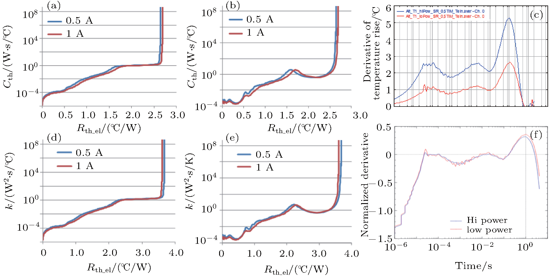 | Fig. 13. Measurement deviation due to noise in the early time range. At 1 A and 0.5 A, the same LED module is measured. Cumulative [(a) and (d)] and derivative structural function [(b) and (e)] ofRth_el and Rth_real are shown. The logarithmic time deviation is depicted before and after normalization [(c) and (f)]. Due to normalization it is revealed that the heat flow through the LED module is identical for both conditions. However, due to the response of the temperature regulation device, differences are visible at 1 s. The larger noise at 0.5 A is visible on the time derivative curves but not on the structural functions. The effect of the noise is clearly visible in the center peak position in the derivative structural functions of Rth_real. The difference of Rth_el and Rth_real is also pronounced. The Rth_el of the 1-A measurement is larger due to the lower WPE at 1 A. However the measurement at 0.5 A has a higher tear-off edge due to the distortion of the active temperature regulation. |
For a white LED with phosphor conversion, another important physical reality needs to be considered, which complicates the interpretation of the structural function. In the Cauer network of Fig. 4, the thermal masses on top of the LED module are excluded, as are the phosphor and the optical glob top or directly attached lenses. The heat source is located on the junction, neglecting that approximately 10% of the heat is generated in the phosphor due to the conversion of blue light into yellow light. The upstream thermal masses also change the heat flux symmetry. In the first time period during heating up, the heat generated in the junction, which has a small thermal capacity, is conducted into the larger upstream thermal masses, which initially are at ambient temperature. The upstream thermal masses heat up and reach the junction’ s temperature. Because heat is also generated in the phosphor, the temperature of the phosphor finally rises above the temperature of the junction. However, during cooling down, the heat flow path is different, i.e. heating up and cooling down curves are not equal anymore: The phosphor temperature is always higher than the junction temperature. The heat is conducted solely upstream to the temperature controlled plate (note: heat transfer by either convection or radiation is neglected).
In Ref. [29] the effect of the phosphor was included in transient FE simulations to analyze the time-resolved temperature data. Recently, further experimental data and RC-network simulation were published.[32] The results are rather devastating for interpretation of the structural function: Without proper modeling of the transient thermal curves, no correct interpretation of the thermal resistance represented by the structural function is possible. The modeling needs as input alongside the proper values for heat capacity, thermal conductivities, and thermal contact resistances, which are for the device’ s components not accessible in standard data bases — the distribution of the thermal load between phosphor and junction.
In the following section, the relative thermal resistance measurement method is applied to reliability investigation of ceramic LED packages on Al-IMS boards, as depicted in Fig. 2. The main results were published recently.[13, 33]
By normalization, the reference to an Rth_real value is lost. However, it can be reestablished by known good reference samples. Another approach is performed in Subsection 4.4 by transient finite element simulation. Changes in the normalized B(ν ) in a certain time range are correlated to an Rth_real increase.
The test samples investigated were high-power ceramic LED packages on Al-IMS. The ceramic carrier material is AlN with typical size between 1.9 mm × 2.3 mm and 1.3 mm × 1.7 mm. Different solder pad footprints are used by the manufacturers, i.e. with or without additional thermal contacts for this kind of packages.
In the present paper, reliability investigations on two different LED packages are presented. Package A, which is depicted in Fig. 2, and package B, depicted in Fig. 14.
 | Fig. 14. Level 2 board under test with footprint and top view of LED ceramic package B. |
The LED packages A were soldered on Al-IMS boards.[13] Two test batches were assembled: one with SAC305 (Sn96.5/Ag3/Cu0.5) and another one with Innolot (Sn91, 175/Ag3, 5/Cu0, 7/Ni0, 125/Sb1, 5/Bi3). Every test group contained 40 LEDs. To eliminate the statistical occurrence of voids in the solder joint, a vacuum solder process was chosen for assembly. Almost void-free solder joints were obtained.
For package B, two parameters are varied within the test batches: 1) The dielectric layer, i.e. its thickness and material properties and 2) the solder material. The samples were assembled using a standard SMD process: The solder paste is printed on the Al-IMS boards, the LEDs are placed on the board followed by reflow in an SMD convection oven. Overall, 240 LEDs were tested, separated into 8 groups, i.e., 30 LEDs per group. Four different Al-IMS and two different solder materials (Eutectic lead tin and Innolot) were tested.
The focus of the investigation was the thermo-mechanical stress induced due to the difference in thermal expansion between the ceramic carrier and the Al-IMS. Passive temperature cycling was performed by placing the LEDs in a temperature shock test (TST) chamber with a temperature setting − 40 ° C/+ 125 ° C; dwell time in the hot and cold conditions was 30 min, respectively, along with a transfer time of 10 s. One cycle is approximately 1 h long.
The transient thermal measurements for package A were taken as described in Subsection 2.4., i.e., 0.7 A was applied for 40 s to ensure thermal equilibrium and then the forward voltage Vf(t) was measured for 40 s using a sense current of 20 mA. The thermal response at initial ‘ 0’ cycles and after ‘ n’ cycles was measured. The measurement time of 40 s is unnecessarily long. For the second test run with test samples B the measurement time was reduced to 5 s.
For the investigation within this paper the focus was set on failures within the LED Level-2 modules. The thermal interface between the Al-IMS and the heat sink was not investigated. In principle, this allowed us to reduce the heating up and cooling down time further to 0.5 s, because data later than 300 ms are not included for data analysis. The shape of the transient signal does not change when cycle of heating up and cooling down times is shortened.
For the test run with package A, the samples were taken out after defined cycle intervals (numbers: 0, 100, 214, 399, 640, 802, 1009, 1500) and measured. For the second test run 500 cycles were completed.
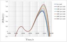
B(ν ) curves of an SAC and an Innolot sample from the first test run are depicted in Fig. 15. The B(ν ) curves of the LEDs have a maximum between 50 ms– 100 ms. The maximum increases with the number of temperature cycles.
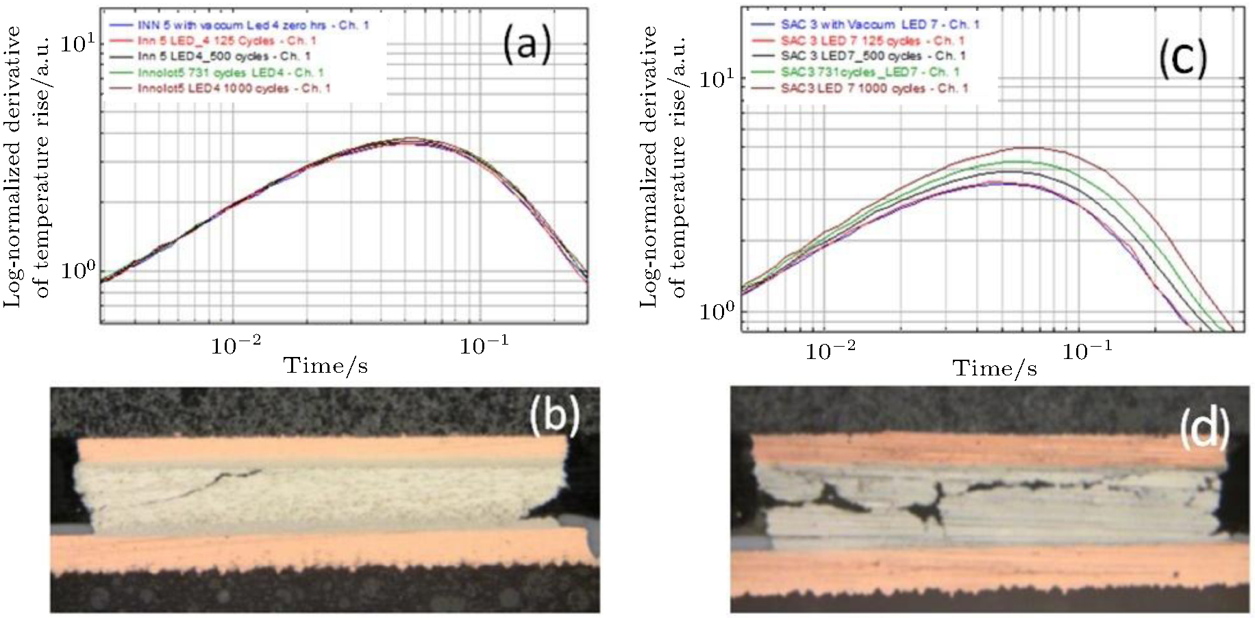 | Fig. 15. Left: log-derivative plot of an Innolot sample at different temperature cycles (a); cross-section of the Innolot sample after 1000 TST cycles (b). Right: log-derivative plot of an SAC sample at different temperature cycles; (c) cross-section of the SAC sample after 1000 TST (d). The peak increase due to the crack in the solder joint is visible in the right figures [(c) and (d)]. |
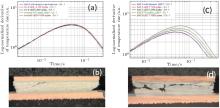
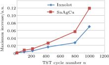
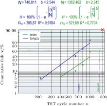
The maximum can be correlated to the solder joint integrity, i.e. cracks within the solder joint, see Fig. 15. The contribution of the thermal resistance due to the dielectric layer contributes to the same peak at almost the same location because the thermal mass of the thin electrical copper layer is small. The delamination of the dielectric layer would also cause a peak increase. However, delamination of the dielectric layer was not observed in the cross sections. Both samples were subjected to 1000 TST cycles and afterward, cross sections were taken. It is remarkable to note that the maximum of the SAC samples increases quicker with TST cycles than the maximum of the Innolot samples does. Cross-sections of the samples after 1000 TST cycles confirmed the experimental results that the SAC samples, which had a larger increase of the maximum, revealed significant cracks while the Innolot samples, with relatively low increase, had fewer noticeable cracks. A complete analysis of all the samples in the test is made and the average of the relative difference in peak height of the normalized log-derivative plot is calculated (see Fig. 16). From Fig. 16, note that the maximum of SAC samples increases more strongly than that of the Innolot samples for every given ‘ n’ cycle number. This is because of better creep resistance of Innolot under the test conditions. Considering an increase of 0.05 in the peak height as failure criterion (which represents an increase of 0.8 ° C/W; see simulation section) cumulative failure distribution and Weibull plots for SAC and Innolot are calculated and depicted in Fig. 17, together with the Weibull parameters. The characteristic lifetime of Innolot is longer (N = 1362 cycles) than that of SAC (N = 740 cycles).
 | Fig. 16. Average peak height increase of Innolot and SAC samples as functions of the cycle number. |
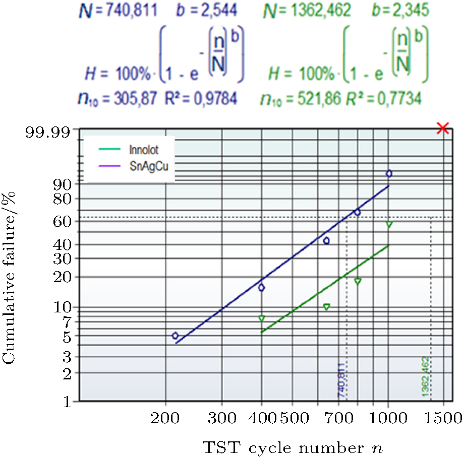 | Fig. 17. Weibull plot of Innolot (R2 = 0.7734) and SAC (R2 = 0.9784). Twenty-four of 40 samples were cycled to 1500 cycles. Red cross indicates 100% failure for both SAC and Innolot samples. |
For 24 samples, the TST tests were continued to 1500 cycles. Light-on failure was observed for only one LED soldered with SAC. Thermal measurements revealed for all samples a large increase of the maximum, and they are all considered to have failed. The linear fit of Innolot is not as good as that for SAC, indicating that different failure mechanisms are operative. The coefficients of determination are R2 = 0.9784 for SAC and R2 = 0.7734 for Innolot. Initially at lower cycles, the Innolot performs better than the SAC solder. However it appears that the failure rate of Innolot increases faster. This behavior was already found for large ceramic carriers on copper heat spreaders.[34]
An FE model (see Fig. 18) was set up in Solid Works using the integrated Flo-EFD solver from Nika (now Mentor Graphics). Our main target was to correlate the peak height of the maximum with the Rth_real increase of the module and to investigate the potential crack which causes the effect. The thermal boundary conditions of the transient temperature measurements are reproduced in the model. The model of the LED package is based on original CAD data. The model size was about 800.000 cells. The multiple, complex, and thin layers of the die are simplified to restrict the level of refinement and number of cells. Only heat conduction is enabled because the heat dissipated by radiation and convection from the LED package and PCB to the ambient air is very small (below 5%) and not relevant for investigating the change of the transient signals due to changes in the solder interconnection. The value of thermal conductivity and heat capacity of the materials were taken from the literature. As thermal boundary condition, a heat flux of Pth = 1.5 W was applied — distributed on the epitaxial layer and the phosphorus. A heat transfer boundary condition P = α · A· (T− 25 ° C) was applied at the bottom of the temperature-controlled plate (α is the heat transfer coefficient, and A is the area of the plate).
 | Fig. 18. Finite element model and simulated temperature distribution of a high power LED test sample with no crack in the solder joint. |
As the initial step of the simulation, a steady state simulation with the thermal load of 1.5 W is performed. The calculated temperature distribution from the steady state simulation is taken as the initial temperature distribution for the transient simulation of the cooling down phase, for which the heat load is switched to zero. The simulated temperature data are post-processed:
TJ = average temperature of the volume representing the epitaxial layer of the junction;
TA = maximum temperature of the temperature-controlled plate = Tcase (temperature below the module).
The Rth_real is obtained from the junction temperature of the initial steady state simulation using Eq. (3). From the time-resolved cooling-down simulation, TJ(t) is extracted and the normalized B(ν ) is calculated.
In the first phases of the simulation, the material parameters of the simplified epitaxial structure were adjusted to match the simulated signal with the experimental one.
After qualitative matching of the experimental curves with the simulated ones in the relevant time domain, i.e., after 1 ms, for zero-hour conditions, the thermal conductivity of the solder material was used as the first parameter to simulate degradation of the solder joint. Stepwise, the thermal conductivity was reduced from the typical value of 56 W/mK for SAC to 5.6 W/mK. This common approach represents the introduction of homogenously distributed very small cracks or voids into the solder joint.
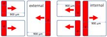
Afterward, cracks were simulated by defining infinite thermal resistance on the bottom of the solder joint as the area of the crack. This can be considered as the most severe condition: The heat transfer is assumed to be fully blocked by the crack area. Two different types of crack location and growth were simulated: (i) crack growing from the outer region of the solder joint toward the center of the package (referred to as external cracks) and (ii) unphysical cracks growing from the inside of the package toward the outer region (referred to as internal cracks), as depicted in Fig. 19. Clearly, external crack growth can be expected because at the outer location the stress is at maximum level. The unphysical internal cracks are simulated solely to evaluate the impact of the crack position on the thermal resistance.
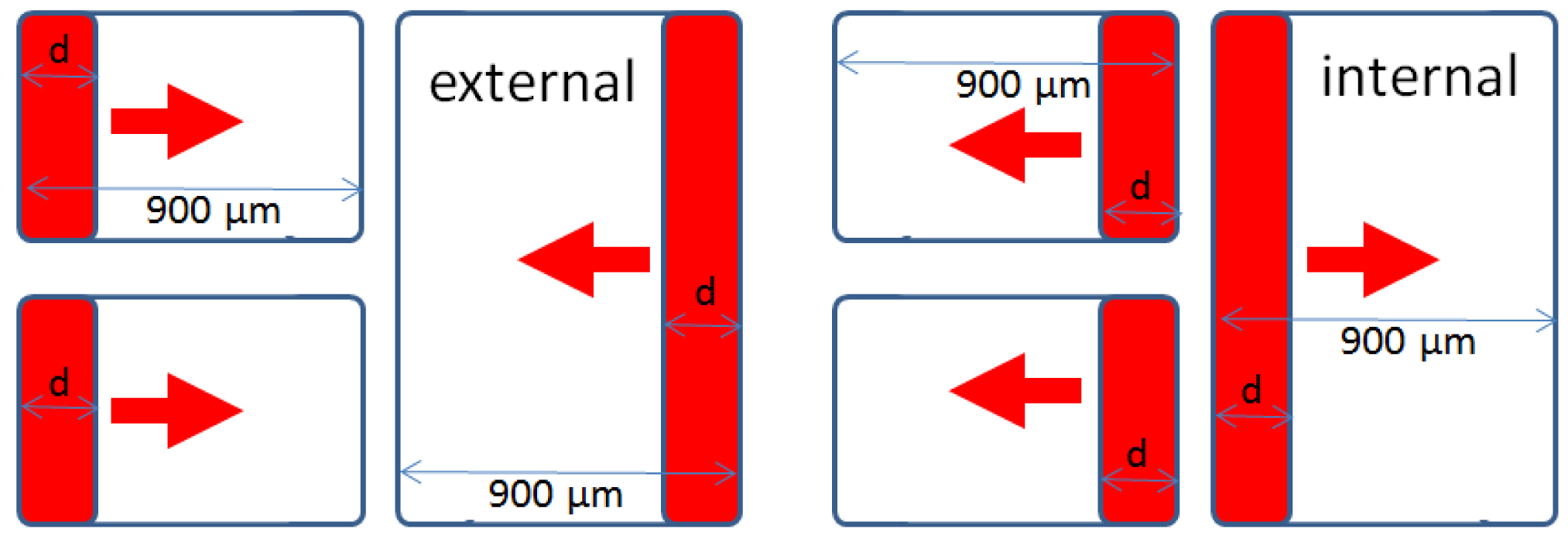 | Fig. 19. Schematic view of the direction of crack development. Red area indicates the crack locations and the corresponding arrows indicate the direction of crack growth. |
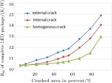
Different crack lengths were simulated, starting from 50-μ m to an almost fully cracked joint with 850-μ m length. The simulated increase of the thermal resistance for the different crack modeling is depicted in Fig. 20. First of all, note that the increase of thermal resistance for external and internal cracks is much greater than the increase caused by homogeneous cracks. The simulated increase of the Rth_real for the homogeneous case matches very well with the increase that is calculated with the one-dimensional Fourier-law for the solder joint: Rth_real_solder = h/(A · λ ), with A the area of the solder joint, h its thickness, and λ the thermal conductivity. In the case of homogeneous cracks, the heat flow path does not change, and only the thermal resistance of the solder joint increases.
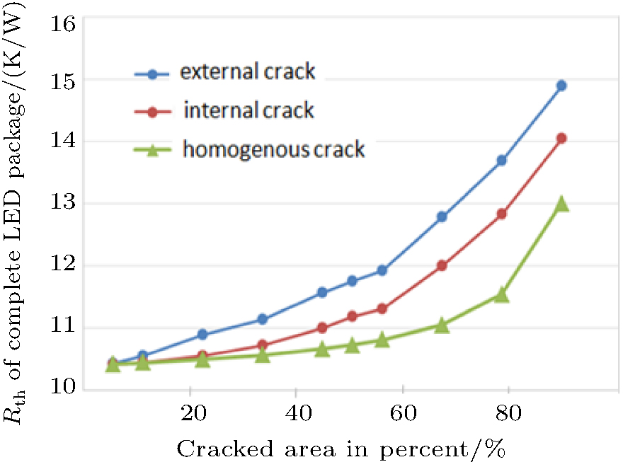 | Fig. 20. Thermal resistance Rth (junction-to-case) of the package versus the cracked area. |
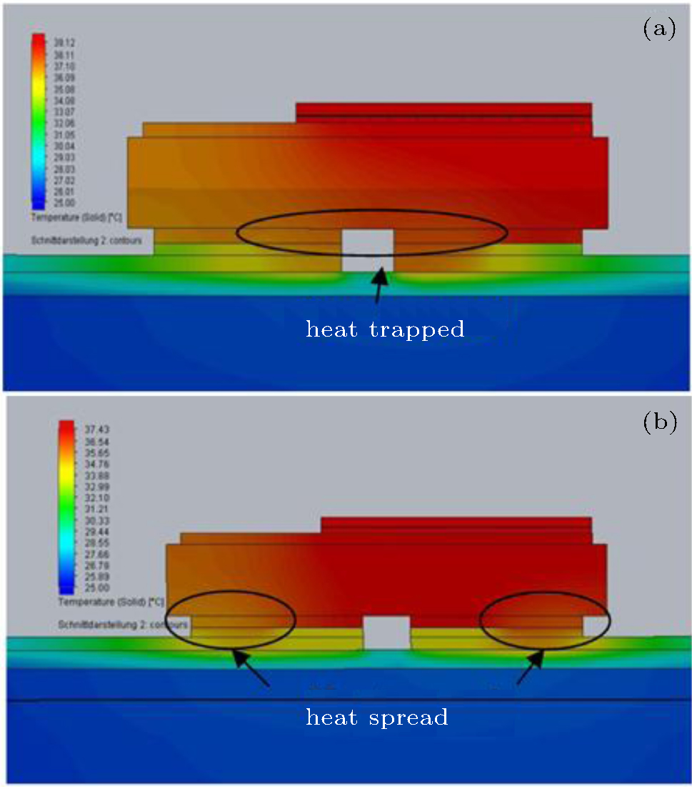
By comparing Figs. 21(a) and 21(b) the difference between external and internal cracks with regard to heat spreading becomes obvious. The effective area available between the electrical pads for heat spreading is reduced as the crack propagates from the exterior region toward the interior. In the case of an external crack, the relative increase of the thermal resistance for small cracks is dominated by the effect of reduction of area for effective heat transfer through the dielectric layer of the Al-IMS. This has to be considered when estimating the cracked area based on experimental data.
 | Fig. 21. (a) FE analysis of internal crack of 450 μ m and (b) FE analysis of external crack of 450 μ m. |
It is interesting to note that for the LED package under investigation, a 25% homogeneously distributed crack causes an increase of only Δ Rth_real ≈ 0.1 K/W, because typically, 25% presence of voids is still accepted in SMD soldering. This increase is actually almost negligible from thermal performance point of view when the cracks are homogeneously distributed. However a large void of 25% in one of the contacts causes a larger thermal impact, due to the reduction of effective area for heat spreading in the Al-IMS (Δ Rth_real ≈ 0.5 K/W). For LED packages with a ceramic heat spreader, the thermal impact of voids in the range of 25% is therefore limited and acceptable. However the impact on reliability can be more severe. Presently, investigations are ongoing to evaluate the impact of initial voids in the solder joint on the crack growth.
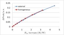
Figure 22 depicts the simulated logarithmic time-derived curves for external cracks. The increase of the maximum between 70 ms– 100 ms is visible, as experimentally observed during the temperature shock test. The increase of peak height from the transient simulation was correlated to the thermal resistance increase obtained by the temperature increase calculated by the steady state simulations for homogenous cracks and external cracks (see Fig. 20). The dependence is almost linear, indicating a direct correlation.
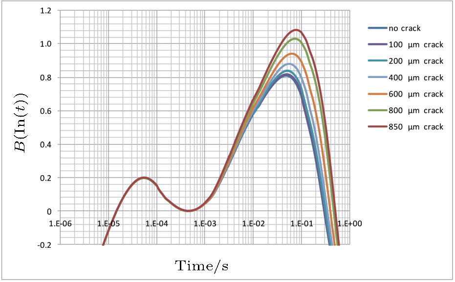 | Fig. 22. Derivative of thermal response with varying external crack lengths. |
Finally, it is possible to estimate the cracked area for the failure criterion “ increase of maximum larger than 0.05.” From Fig. 16 we get for “ 0.05 maximum increase” an Rth_real increase of 0.8 K/W. For external cracks, from Fig. 23 we obtain a crack length of 300 μ m. For homogeneously distributed voids, a cracked area of roughly 70% is obtained. However, in the FE simulation, the cracked area is fully thermally insulating, which will not be the case in reality. Therefore, the cracked area will be slightly larger, and the 33% can be considered to be the lower limit.
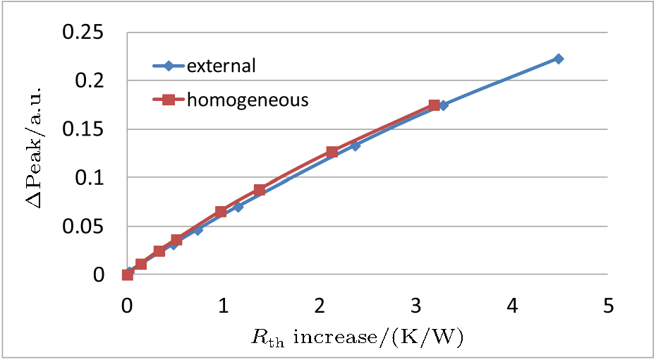 | Fig. 23. Increase of maximum between 50 ms– 100 ms, dependent upon the increase in Rth_real. |
For the LED packages B, differences among the LEDs are already observed at 0-hour testing. They occur at two different time ranges and are called failure modes in the following. The first failure mode is “ peak height” of the peak, which occurs at 30 ms. The second failure mode, “ saddle height” occurs at 1 ms. The two failure modes are depicted in Fig. 24. The first failure mode occurs in the time domain when the heat flows from the ceramic carrier to the board, e.g., solder contact and dielectric layer. The second failure mode occurs when the heat flows into the ceramic carrier. Changes in the saddle height indicate failures on the die level. It is remarkable that within a batch of test samples at 0-hours the “ saddle height” and “ peak height” both vary. For zero-hour inline inspection, one uses a golden reference sample and defines a distinct deviation from the reference sample as a failure. The peak in the B(ν ) curve occurs at a time when the temperature gradient between ceramic carriers and the Al-core of the IMS decays. The height is determined by the thermal resistance of the solder joint and the dielectric layer, i.e., the thermal resistance between the ceramic and the Al-core. Whether the contributions can be separated depends on the thermal mass of the copper electric layer of the IMS. The variation of the peak height at zero hour is due to the LED position (different heat spreading due to pad layout and drillings) and due to production variations within the dielectric layer. Also initial voiding in the solder joint increases the peak height. Therefore, the assemblies were inspected by x-ray, and the variation of voids was less than 20%. With Fourier’ s law, the thermal resistance Rth_real_solder of the solder joint can be estimated (using the footprint in Fig. 14, and assuming a typical solder joint thickness of 50 μ m and a thermal conduction of 56 W/mK of the tin solder results in Rth_real_solder = 0.75 K/W). When the solder joint has 20% homogeneously distributed voids, the area of the solder joint is reduced to 80% and the thermal resistance increases: Δ Rth_real_solder < 0.2 K/W. This value is hardly detectable in the structural function. By finite element simulation, a Δ Rth_real = 0.2 K/W induces a peak increase of 0.0125. This peak increase is resolved in the normalized B(ν ), indicating an increase of resolution due to the relative thermal resistance measurement.
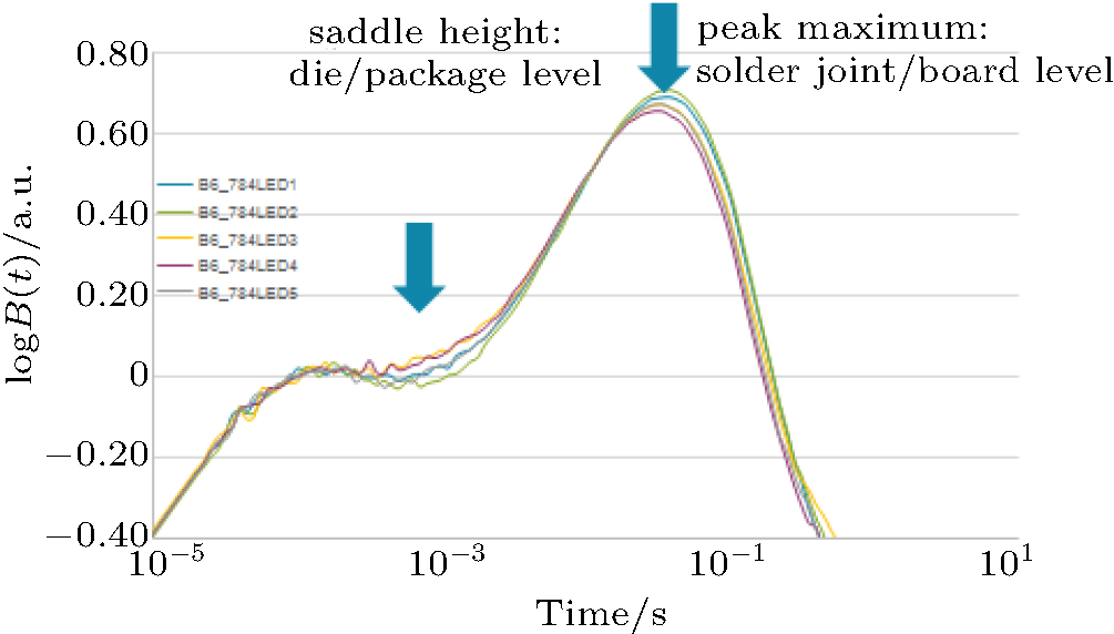 | Fig. 24. Failure mode “ peak height” and failure mode “ saddle height” for a set of LEDs on one IMS board. |
The precise root cause for the saddle height is still under evaluation: The die interconnection between the LED and the ceramic is most reasonable. However, the attachment of the phosphorus to the die also influences the signal in this time domain.
So far, 500 temperature cycles were executed for LED type B. No changes in the saddle height had been observed during the temperature shock test up to 500 cycles, indicating that no failures on the die and package levels occurred. In contrast, the peak height increases. The average increase is depicted in Table 1. The difference of the thermal degradation, dependent upon the Al-IMS and the solder material is significant. Board A is an IMS with a very thin dielectric layer for excellent thermal performance. However for both solder materials, strong thermal degradation is observed, indicating either solder joint cracking or delamination of the dielectric layer. For the first test run, delamination of the dielectric layer of the Al-IMS was not observed. For the second test batch, further evaluation is ongoing, i.e., the separation between the potential failure mode dielectric layer delamination and solder joint cracking.
| Table 1. Average peak increase occurring for the different batches. The error of the mean average is in the range of 0.002. |
Transient thermal analysis of relative thermal resistance is a sensitive tool to detect and separate failures in LED packages. The approach to analyzing relative thermal resistance reduces measurement effort and increases sensitivity. Depending on the focus of the analysis, the measurement time can be reduced to 0.5 s and even lower. For dedicated testing of the first level interconnect, i.e. the die interconnect, very short measurement times of 50 ms are sufficient. The measurement of the relative thermal resistance has the potential to close the gap between simple electric resistance measurement and the more advanced thermal resistance measurement that provides much more information for failure analysis of high-power LEDs.
The developed data processing algorithms enable automatic data evaluation. High volume testing in production of the thermal path and separation of failure modes can be implemented. Both accurate reliability testing and lifetime prediction can be accomplished.
The authors would like to thank the AutoLED Competence Team of Philips GmbH in Aachen for cooperation, especially Benno Spinger, Nils Benter, Robert Derix, Udo Karbowski, Rob Einig, Astrid Marchewka, Michael Deckers, Harry Gijsbers, Adam Lind, Nico Bienen, and Harald Willwohl.
| 1 |
|
| 2 |
|
| 3 |
|
| 4 |
|
| 5 |
|
| 6 |
|
| 7 |
|
| 8 |
|
| 9 |
|
| 10 |
|
| 11 |
|
| 12 |
|
| 13 |
|
| 14 |
|
| 15 |
|
| 16 |
|
| 17 |
|
| 18 |
|
| 19 |
|
| 20 |
|
| 21 |
|
| 22 |
|
| 23 |
|
| 24 |
|
| 25 |
|
| 26 |
|
| 27 |
|
| 28 |
|
| 29 |
|
| 30 |
|
| 31 |
|
| 32 |
|
| 33 |
|
| 34 |
|