|
|
|
Interfaces between MoOx and MoX2 (X = S, Se, and Te) |
| Fengming Chen(陈凤鸣)1, Jinxin Liu(刘金鑫)1, Xiaoming Zheng(郑晓明)1, Longhui Liu(刘龙慧)1, Haipeng Xie(谢海鹏)1, Fei Song(宋飞)2, Yongli Gao(高永立)3,1, and Han Huang(黄寒)1, † |
1 Hunan Key Laboratory of Super-microstructure and Ultrafast Process, School of Physics and Electronics, Central South University, Changsha 410083, China
2 Shanghai Synchrotron Radiation Facility, Shanghai Institute of Applied Physics, Chinese Academy of Sciences, Shanghai 201204, China
3 Department of Physics and Astronomy, University of Rochester, Rochester, NY 14627, USA |
|
|
|
|
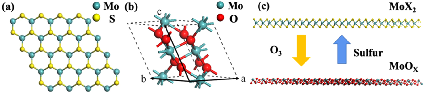
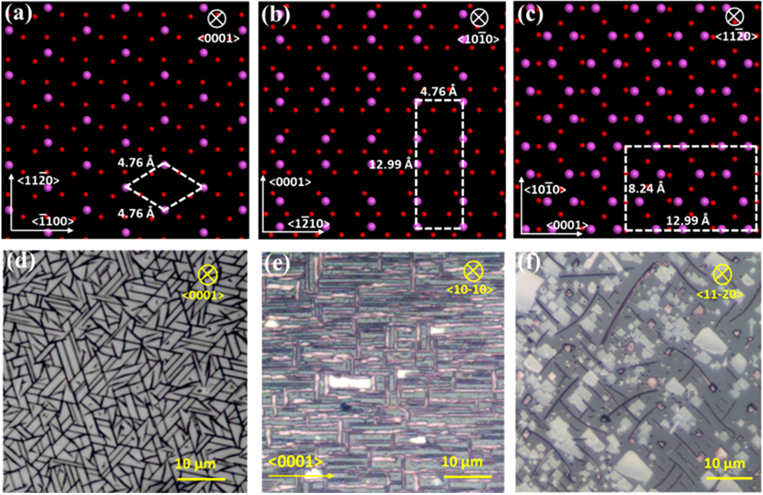
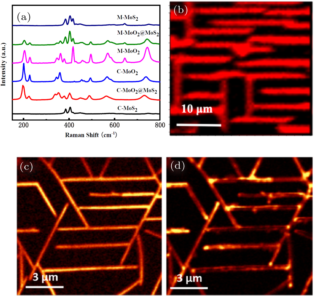
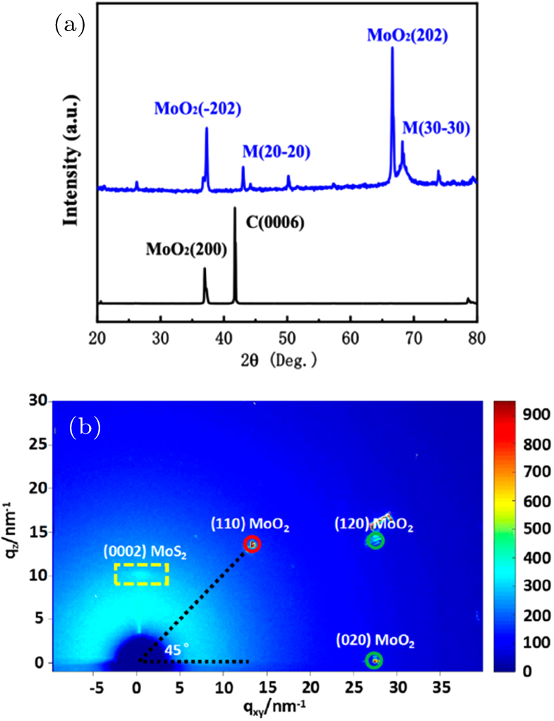
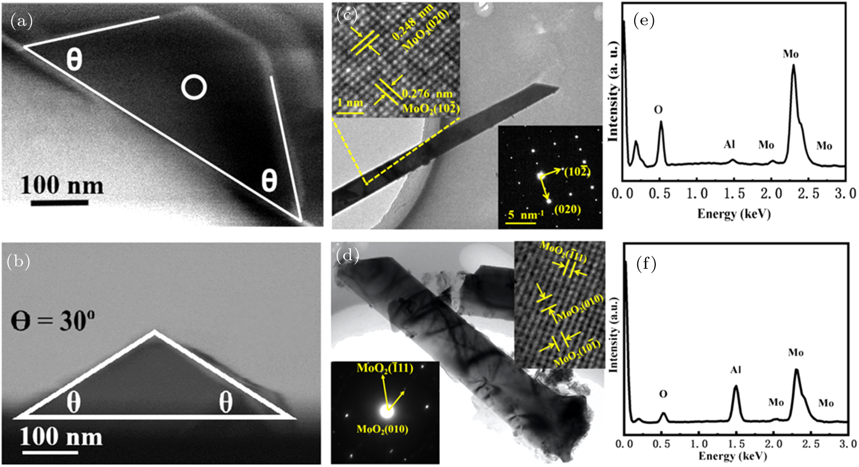
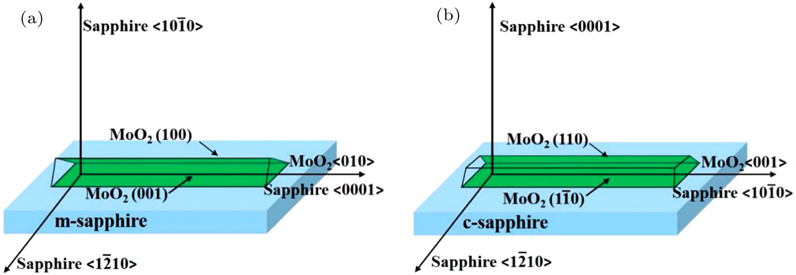
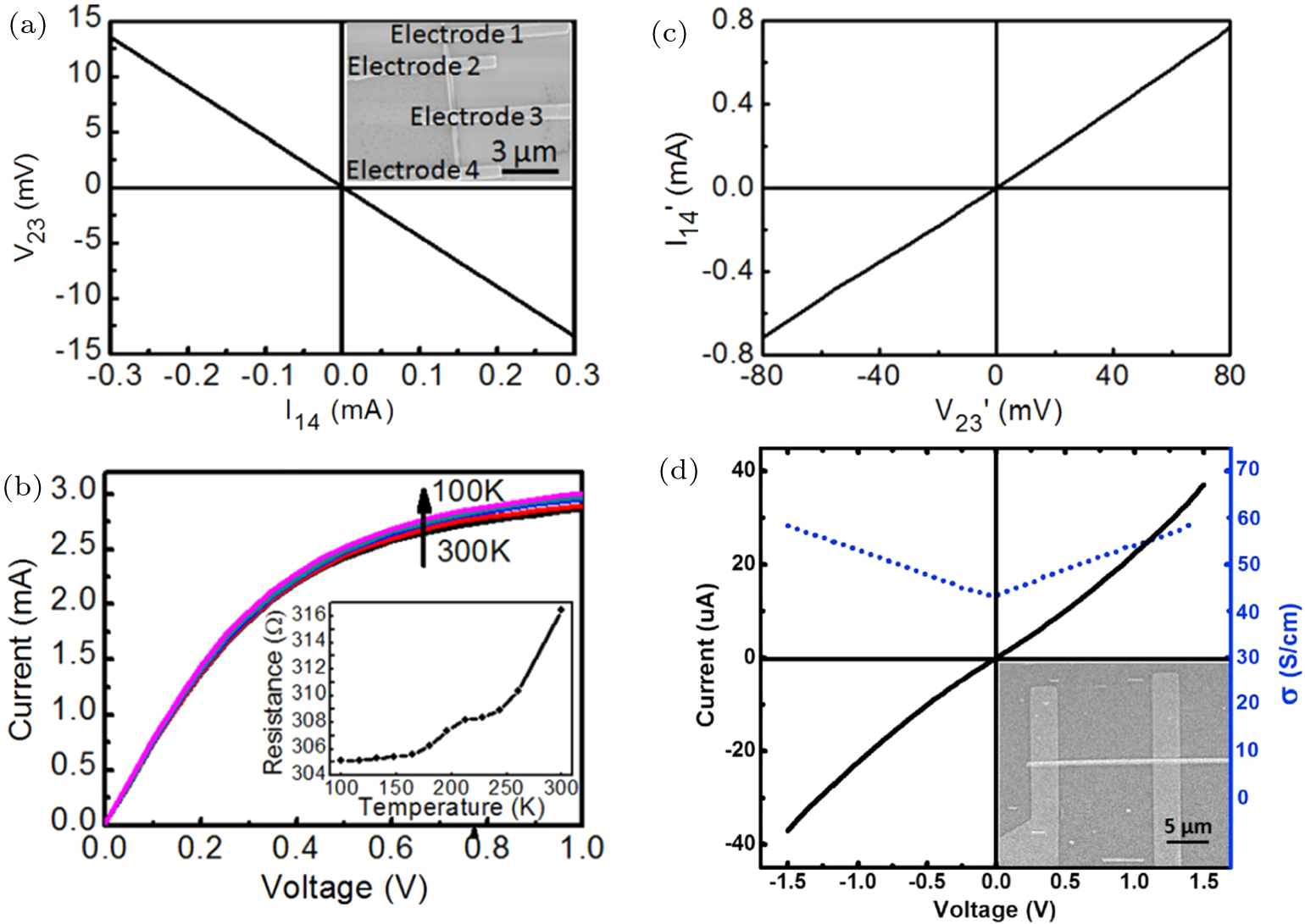
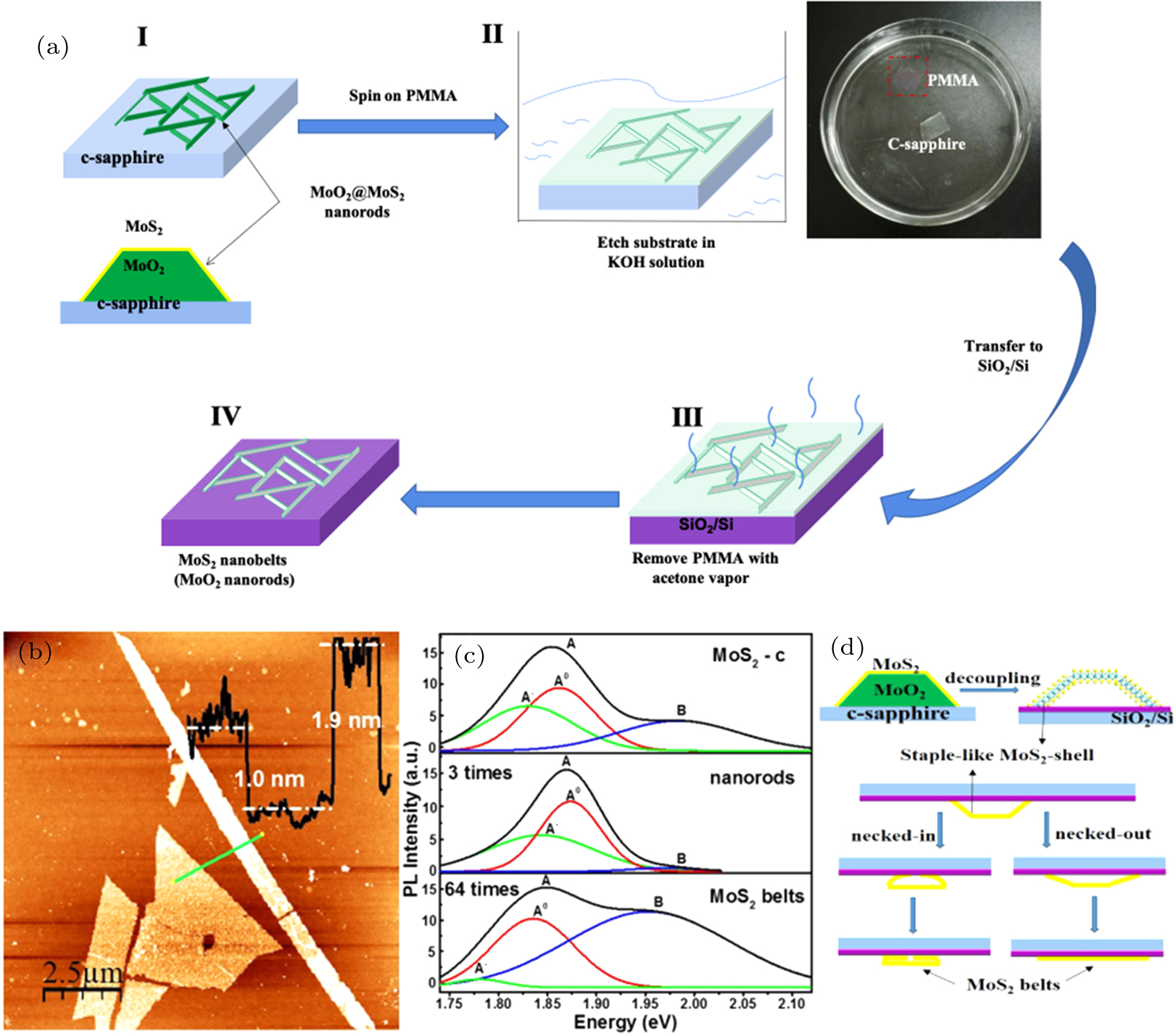
Abstract In the past decades there have been many breakthroughs in low-dimensional materials, especially in two-dimensional (2D) atomically thin crystals like graphene. As structural analogues of graphene but with a sizeable band gap, monolayers of atomically thin transition metal dichalcogenides (with formula of MX2, M = Mo, W; X = S, Se, Te, etc.) have emerged as the ideal 2D prototypes for exploring fundamentals in physics such as valleytronics due to the quantum confinement effects, and for engineering a wide range of nanoelectronic, optoelectronic, and photocatalytic applications. Transition metal trioxides as promising materials with low evaporation temperature, high work function, and inertness to air have been widely used in the fabrication and modification of MX2. In this review, we reported the fabrications of one-dimensional MoS2 wrapped MoO2 single crystals with varied crystal direction via atmospheric pressure chemical vapor deposition method and of 2D MoOx covered MoX2 by means of exposing MoX2 to ultraviolet ozone. The prototype devices show good performances. The approaches are common to other transition metal dichalcogenides and transition metal oxides.
|
Received: 08 July 2020
Revised: 10 August 2020
Accepted manuscript online: 27 August 2020
|
| Fund: the National Natural Science Foundation of China (Grant No. 11874427), the National Science Foundation DMR-1903962, and the Fundamental Research Funds for the Central Universities of Central South University (Grant No. 2019zzts429). |
|
Corresponding Authors:
†Corresponding author. E-mail: physhh@csu.edu.cn
|
Cite this article:
Fengming Chen(陈凤鸣), Jinxin Liu(刘金鑫), Xiaoming Zheng(郑晓明), Longhui Liu(刘龙慧), Haipeng Xie(谢海鹏), Fei Song(宋飞), Yongli Gao(高永立), and Han Huang(黄寒) Interfaces between MoOx and MoX2 (X = S, Se, and Te) 2020 Chin. Phys. B 29 116802
|
| [1] |
|
| [2] |
|
| [3] |
Tan C, Cao X, Wu X J, He Q, Yang J, Zhang X, Chen J, Zhao W, Han S, Nam G H, Sindoro M, Zhang H 2017 Chem. Rev. 117 6225 DOI: 10.1021/acs.chemrev.6b00558 |
| [4] |
|
| [5] |
Wang Q H, Kalantar-Zadeh K, Kis A, Coleman J N, Strano M S 2012 Nat. Nanotechnol. 7 699 DOI: 10.1038/nnano.2012.193 |
| [6] |
|
| [7] |
|
| [8] |
Novoselov K S, Jiang D, Schedin F, Booth T, Khotkevich V, Morozov S, Geim A K 2005 Proc. Natl. Acad. Sci. USA 102 10451 DOI: 10.1073/pnas.0502848102 |
| [9] |
Jo I, Pettes M T, Kim J, Watanabe K, Taniguchi T, Yao Z, Shi L 2013 Nano Lett. 13 550 DOI: 10.1021/nl304060g |
| [10] |
|
| [11] |
|
| [12] |
Jariwala D, Sangwan V K, Lauhon L J, Marks T J, Hersam M C 2014 ACS Nano 8 1102 DOI: 10.1021/nn500064s |
| [13] |
Koenig S P, Doganov R A, Schmidt H, Castro Neto A, Özyilmaz B 2014 Appl. Phys. Lett. 104 103106 DOI: 10.1063/1.4868132 |
| [14] |
Castellanos-Gomez A, Vicarelli L, Prada E, Island J O, Narasimha-Acharya K, Blanter S I, Groenendijk D J, Buscema M, Steele G A, Alvarez J 2014 2D Mater. 1 025001 DOI: 10.1088/2053-1583/1/2/025001 |
| [15] |
|
| [16] |
|
| [17] |
Tao L, Cinquanta E, Chiappe D, Grazianetti C, Fanciulli M, Dubey M, Molle A, Akinwande D 2015 Nat. Nanotechnol. 10 227 DOI: 10.1038/nnano.2014.325 |
| [18] |
Ni Z, Liu Q, Tang K, Zheng J, Zhou J, Qin R, Gao Z, Yu D, Lu J 2012 Nano Lett. 12 113 DOI: 10.1021/nl203065e |
| [19] |
|
| [20] |
Wang H, Yu L, Lee Y H, Shi Y, Hsu A, Chin M L, Li L J, Dubey M, Kong J, Palacios T 2012 Nano Lett. 12 4674 DOI: 10.1021/nl302015v |
| [21] |
|
| [22] |
Jiang J, Hu W, Xie D, Yang J, He J, Gao Y, Wan Q 2019 Nanoscale 11 1360 DOI: 10.1039/C8NR07133K |
| [23] |
|
| [24] |
Pu J, Yomogida Y, Liu K K, Li L J, Iwasa Y, Takenobu T 2012 Nano Lett. 12 4013 DOI: 10.1021/nl301335q |
| [25] |
Yin Z, Li H, Li H, Jiang L, Shi Y, Sun Y, Lu G, Zhang Q, Chen X, Zhang H 2011 ACS Nano 6 74 DOI: 10.1021/nn2024557 |
| [26] |
Zhang W, Huang J K, Chen C H, Chang Y H, Cheng Y J, Li L J 2013 Adv. Mater. 25 3456 DOI: 10.1002/adma.v25.25 |
| [27] |
Roy K, Padmanabhan M, Goswami S, Sai T P, Ramalingam G, Raghavan S, Ghosh A 2013 Nat. Nanotechnol. 8 826 DOI: 10.1038/nnano.2013.206 |
| [28] |
Yu L, Lee Y H, Ling X, Santos E J, Shin Y C, Lin Y, Dubey M, Kaxiras E, Kong J, Wang H 2014 Nano Lett. 14 3055 DOI: 10.1021/nl404795z |
| [29] |
Lee G H, Yu Y J, Cui X, Petrone N, Lee C H, Choi M S, Lee D Y, Lee C, Yoo W J, Watanabe K 2013 ACS Nano 7 7931 DOI: 10.1021/nn402954e |
| [30] |
Baugher B W, Churchill H O, Yang Y, Jarillo-Herrero P 2013 Nano Lett. 13 4212 DOI: 10.1021/nl401916s |
| [31] |
Schmidt H, Wang S, Chu L, Toh M, Kumar R, Zhao W, Neto A H, Martin J, Adam S, Özyilmaz B, Eda G 2014 Nano Lett. 14 1909 DOI: 10.1021/nl4046922 |
| [32] |
|
| [33] |
|
| [34] |
Wang Q, Lei Y, Wang Y, Liu Y, Song C, Zeng J, Song Y, Duan X, Wang D, Li Y 2020 Energy Environ. Sci. 13 1593 DOI: 10.1039/D0EE00450B |
| [35] |
Fang L, Chen H, Yuan X, Huang H, Chen G, Li L, Ding J, He J, Tao S 2019 Nanoscale Res. Lett. 14 274 DOI: 10.1186/s11671-019-3110-z |
| [36] |
Jiang J, Li N, Zou J, Zhou X, Eda G, Zhang Q, Zhang H, Li L-J, Zhai T, Wee A T 2019 Chem. Soc. Rev. 48 4639 DOI: 10.1039/C9CS00348G |
| [37] |
Fang L, Yuan X, Liu K, Li L, Zhou P, Ma W, Huang H, He J, Tao S 2020 Nanoscale 12 3715 DOI: 10.1039/C9NR09874G |
| [38] |
|
| [39] |
|
| [40] |
Kang K, Xie S, Huang L, Han Y, Huang P Y, Mak K F, Kim C J, Muller D, Park J 2015 Nature 520 656 DOI: 10.1038/nature14417 |
| [41] |
Tongay S, Fan W, Kang J, Park J, Koldemir U, Suh J, Narang D S, Liu K, Ji J, Li J 2014 Nano Lett. 14 3185 DOI: 10.1021/nl500515q |
| [42] |
|
| [43] |
Ouyang F, Yang Z, Ni X, Wu N, Chen Y, Xiong X 2014 Appl. Phys. Lett. 104 071901 DOI: 10.1063/1.4865902 |
| [44] |
Kosynkin D V, Higginbotham A L, Sinitskii A, Lomeda J R, Dimiev A, Price B K, Tour J M 2009 Nature 458 872 DOI: 10.1038/nature07872 |
| [45] |
|
| [46] |
Li S, Lin Y C, Zhao W, Wu J, Wang Z, Hu Z, Shen Y, Tang D M, Wang J, Zhang Q 2018 Nat. Mater. 17 535 DOI: 10.1038/s41563-018-0055-z |
| [47] |
Zhou D, Li H, Si N, Jiang Y, Huang H, Li H, Niu T 2020 Appl. Phys. Lett. 116 061602 DOI: 10.1063/1.5140376 |
| [48] |
|
| [49] |
Kang L, Chen H, Yang Z J, Yuan Y, Huang H, Yang B, Gao Y, Zhou C 2018 J. Appl. Phys. 123 205110 DOI: 10.1063/1.5027541 |
| [50] |
|
| [51] |
|
| [52] |
Cai J, Ruffieux P, Jaafar R, Bieri M, Braun T, Blankenburg S, Muoth M, Seitsonen A P, Saleh M, Feng X 2010 Nature 466 470 DOI: 10.1038/nature09211 |
| [53] |
Ruffieux P, Wang S, Yang B, Sánchez-Sánchez C, Liu J, Dienel T, Talirz L, Shinde P, Pignedoli C A, Passerone D 2016 Nature 531 489 DOI: 10.1038/nature17151 |
| [54] |
|
| [55] |
|
| [56] |
|
| [57] |
|
| [58] |
|
| [59] |
|
| [60] |
|
| [61] |
Meyer J, Kidambi P R, Bayer B C, Weijtens C, Kuhn A, Centeno A, Pesquera A, Zurutuza A, Robertson J, Hofmann S 2014 Sci. Rep. 4 5380 DOI: 10.1038/srep05380 |
| [62] |
|
| [63] |
Lin J D, Han C, Wang F, Wang R, Xiang D, Qin S, Zhang X-A, Wang L, Zhang H, Wee A T S 2014 ACS Nano 8 5323 DOI: 10.1021/nn501580c |
| [64] |
|
| [65] |
Xiang D, Han C, Wu J, Zhong S, Liu Y, Lin J, Zhang X A, Hu W P, Ozyilmaz B, Neto A C 2015 Nat. Commun. 6 6485 DOI: 10.1038/ncomms7485 |
| [66] |
|
| [67] |
Gwinner M C, Pietro R D, Vaynzof Y, Greenberg K J, Ho P K, Friend R H, Sirringhaus H 2011 Adv. Funct. Mater. 21 1432 DOI: 10.1002/adfm.v21.8 |
| [68] |
|
| [69] |
Zhang M, Irfan Ding H, Gao Y, Tang C W 2010 Appl. Phys. Lett. 96 183301 DOI: 10.1063/1.3415497 |
| [70] |
|
| [71] |
|
| [72] |
Wang C, Irfan I, Liu X, Gao Y 2014 J. Vac. Sci. Technol. B 32 040801 DOI: 10.1116/1.4886364 |
| [73] |
Irfan I, James Turinske A, Bao Z, Gao Y 2012 Appl. Phys. Lett. 101 093305 DOI: 10.1063/1.4748978 |
| [74] |
Choi S, Fuentes-Hernandez C, Wang C-Y, Khan T M, Larrain F A, Zhang Y, Barlow S, Marder S R, Kippelen B 2016 ACS Appl. Mater. Interfaces 8 24744 DOI: 10.1021/acsami.6b07029 |
| [75] |
Zhou C, Zhao Y, Raju S, Wang Y, Lin Z, Chan M, Chai Y 2016 Adv. Funct. Mater. 26 4223 DOI: 10.1002/adfm.v26.23 |
| [76] |
Meyer J, Hamwi S, Kröger M, Kowalsky W, Riedl T, Kahn A 2012 Adv. Mater. 24 5408 DOI: 10.1002/adma.v24.40 |
| [77] |
Ho P H, Chang Y R, Chu Y C, Li M K, Tsai C A, Wang W H, Ho C H, Chen C W, Chiu P W 2017 ACS Nano 11 7362 DOI: 10.1021/acsnano.7b03531 |
| [78] |
Yamamoto M, Dutta S, Aikawa S, Nakaharai S, Wakabayashi K, Fuhrer M S, Ueno K, Tsukagoshi K 2015 Nano Lett. 15 2067 DOI: 10.1021/nl5049753 |
| [79] |
Wu D, Yang Y, Zhu P, Zheng X, Chen X, Shi J, Song F, Gao X, Zhang X, Ouyang F, Xiong X, Gao Y, Huang H 2018 J. Phys. Chem. C 122 1860 DOI: 10.1021/acs.jpcc.7b10666 |
| [80] |
Liu J, Shi J, Wu D, Zheng X, Chen F, Xiao J, Li Y, Song F, Gao Y, Huang H 2020 Curr. Appl. Phys. 20 1130 DOI: 10.1016/j.cap.2020.07.015 |
| [81] |
Xie Q, Zheng X, Wu D, Chen X, Shi J, Han X, Zhang X, Peng G, Gao Y, Huang H 2017 Appl. Phys. Lett. 111 093505 DOI: 10.1063/1.5001183 |
| [82] |
Shi J, Wu D, Zheng X, Xie D, Song F, Zhang X, Jiang J, Yuan X, Gao Y, Huang H 2018 Phys. Status Solidi (B) 255 1800254 DOI: 10.1002/pssb.v255.9 |
| [83] |
Wu D, Shi J, Zheng X, Liu J, Dou W, Gao Y, Yuan X, Ouyang F, Huang H 2019 Phys Status Solidi Rapid Res Lett 13 1900063 DOI: 10.1002/pssr.v13.7 |
| [84] |
Zheng X, Wei Y, Deng C, Huang H, Yu Y, Wang G, Peng G, Zhu Z, Zhang Y, Jiang T, Qin S, Zhang R, Zhang X 2018 ACS Appl. Mater. Interfaces 10 30045 DOI: 10.1021/acsami.8b11003 |
| [85] |
Zheng X, Wei Y, Liu J, Wang S, Shi J, Yang H, Peng G, Deng C, Luo W, Zhao Y, Li Y, Sun K, Wan W, Xie H, Gao Y, Zhang X, Huang H 2019 Nanoscale 11 13469 DOI: 10.1039/C9NR04212A |
| [86] |
Zheng X, Zhang X, Wei Y, Liu J, Yang H, Zhang X, Wang S, Xie H, Deng C, Gao Y 2020 Nano Res. 13 952 DOI: 10.1007/s12274-020-2724-x |
| [87] |
|
| [88] |
|
| [89] |
|
| [90] |
|
| [91] |
Qian F, Gradecak S, Li Y, Wen C-Y, Lieber C M 2005 Nano Lett. 5 2287 DOI: 10.1021/nl051689e |
| [92] |
Mariani G, Zhou Z, Scofield A, Huffaker D L 2013 Nano Lett. 13 1632 DOI: 10.1021/nl400083g |
| [93] |
Chen G, Ågren H, Ohulchanskyy T Y, Prasad P N 2015 Chem. Soc. Rev. 44 1680 DOI: 10.1039/C4CS00170B |
| [94] |
|
| [95] |
|
| [96] |
|
| [97] |
|
| [98] |
Yang T H, Aggarwal R, Gupta A, Zhou H, Narayan R J, Narayan J 2010 J. Appl. Phys. 107 053514 DOI: 10.1063/1.3327241 |
| [99] |
|
| [100] |
Zhao Y, Hwan Lee J, Zhu Y, Nazari M, Chen C, Wang H, Bernussi A, Holtz M, Fan Z 2012 J. Appl. Phys. 111 053533 DOI: 10.1063/1.3692391 |
| [101] |
Baker T J, Haskell B A, Wu F, Speck J S, Nakamura S 2006 Jpn. J. Appl. Phys. 45 L154 DOI: 10.1143/JJAP.45.L154 |
| [102] |
|
| [103] |
Wang S, Rong Y, Fan Y, Pacios M, Bhaskaran H, He K, Warner J H 2014 Chem. Mater. 26 6371 DOI: 10.1021/cm5025662 |
| [104] |
|
| [105] |
|
| [106] |
|
| [107] |
Dieterle M, Weinberg G, Mestl G 2002 Phys. Chem. Chem. Phys. 4 812 DOI: 10.1039/b107012f |
| [108] |
|
| [109] |
Mukundan S, Mohan L, Chandan G, Roul B, Krupanidhi S 2014 J. Appl. Phys. 116 204502 DOI: 10.1063/1.4902892 |
| [110] |
Pu E, Liu D, Ren P, Zhou W, Tang D, Xiang B, Wang Y, Miao J 2017 AIP Adv. 7 025015 DOI: 10.1063/1.4977543 |
| [111] |
|
| [112] |
|
| [113] |
Ahn E, Seo Y S, Cho J, Lee I, Hwang J, Jeen H 2016 RSC Adv. 6 60704 DOI: 10.1039/C6RA09928A |
| [114] |
Dahl-Petersen C, Šarić M, Brorson M, Moses P G, Rossmeisl J, Lauritsen J V, Helveg S 2018 ACS Nano 12 5351 DOI: 10.1021/acsnano.8b00125 |
| [115] |
|
| [116] |
Van Der Zande A M, Huang P Y, Chenet D A, Berkelbach T C, You Y, Lee G H, Heinz T F, Reichman D R, Muller D A, Hone J C 2013 Nat. Mater. 12 554 DOI: 10.1038/nmat3633 |
| [117] |
Li M Y, Shi Y, Cheng C C, Lu L S, Lin Y C, Tang H L, Tsai M L, Chu C W, Wei K H, He J H 2015 Science 349 524 DOI: 10.1126/science.aab4097 |
| [118] |
Endo R, Maeda S, Jinnai Y, Lan R, Kuwahara M, Kobayashi Y, Susa M 2010 Jpn. J. Appl. Phys. 49 065802 DOI: 10.1143/JJAP.49.065802 |
| [119] |
|
| [120] |
Ebbesen T, Lezec H, Hiura H, Bennett J, Ghaemi H, Thio T 1996 Nature 382 54 DOI: 10.1038/382054a0 |
| [121] |
|
| [122] |
Ayari A, Cobas E, Ogundadegbe O, Fuhrer M S 2007 J. Appl. Phys. 101 014507 DOI: 10.1063/1.2407388 |
| [123] |
Conley H J, Wang B, Ziegler J I, Haglund Jr R F, Pantelides S T, Bolotin K I 2013 Nano Lett. 13 3626 DOI: 10.1021/nl4014748 |
| [124] |
|
| [125] |
|
| [126] |
|
| [127] |
|
| [128] |
Qian M Y, Yu Z L, Wan Q, He P B, Liu B, Yang J L, Xu C M, Cai M Q 2020 Phys. Status Solidi Rapid Res. Lett. 14 2000016 DOI: 10.1002/pssr.v14.7 |
| [129] |
|
| [130] |
Das T, Seo D, Seo J E, Chang J 2020 Adv. Electron. Mater. 6 2000008 DOI: 10.1002/aelm.v6.5 |
| [131] |
Hoffman A N, Gu Y, Tokash J, Woodward J, Xiao K, Rack P D 2020 ACS Appl. Mater. Interfaces 12 7345 DOI: 10.1021/acsami.9b21287 |
| [132] |
Lezama I G, Arora A, Ubaldini A, Barreteau C, Giannini E, Potemski M, Morpurgo A F 2015 Nano Lett. 15 2336 DOI: 10.1021/nl5045007 |
| [133] |
Yamamoto M, Wang S T, Ni M, Lin Y F, Li S L, Aikawa S, Jian W B, Ueno K, Wakabayashi K, Tsukagoshi K 2014 ACS Nano 8 3895 DOI: 10.1021/nn5007607 |
| [134] |
Das S, Chen H Y, Penumatcha A V, Appenzeller J 2013 Nano Lett. 13 100 DOI: 10.1021/nl303583v |
| [135] |
|
| [136] |
Sze S M, Ng K K 2006 Physics of semiconductor devices John wiley & sons 135
|
| [137] |
Liu Y, Cai Y, Zhang G, Zhang Y W, Ang K W 2017 Adv. Funct. Mater. 27 1604638 DOI: 10.1002/adfm.v27.7 |
| [138] |
Xia J, Huang X, Liu L Z, Wang M, Wang L, Huang B, Zhu D D, Li J J, Gu C Z, Meng X M 2014 Nanoscale 6 8949 DOI: 10.1039/C4NR02311K |
| No Suggested Reading articles found! |
|
|
Viewed |
|
|
|
Full text
|
|
|
|
|
Abstract
|
|
|
|
|
Cited |
|
|
|
|
Altmetric
|
|
blogs
Facebook pages
Wikipedia page
Google+ users
|
Online attention
Altmetric calculates a score based on the online attention an article receives. Each coloured thread in the circle represents a different type of online attention. The number in the centre is the Altmetric score. Social media and mainstream news media are the main sources that calculate the score. Reference managers such as Mendeley are also tracked but do not contribute to the score. Older articles often score higher because they have had more time to get noticed. To account for this, Altmetric has included the context data for other articles of a similar age.
View more on Altmetrics
|
|
|