| CONDENSED MATTER: ELECTRONIC STRUCTURE, ELECTRICAL, MAGNETIC, AND OPTICAL PROPERTIES |
Prev
Next
|
|
|
Simulation study of device physics and design of GeOI TFET with PNN structure and buried layer for high performance |
| Bin Wang(王斌)1,†, Sheng Hu(胡晟)1, Yue Feng(冯越)1, Peng Li(李鹏)2, Hui-Yong Hu(胡辉勇)1, and Bin Shu(舒斌)1 |
1 State Key Discipline Laboratory of Wide Bandgap Semiconductor Technology, School of Microelectronics, Xidian University, Xi’an 710071, China
2 Xi’an Microelectronic Technology Institute, Xi’an 710054, China |
|
|
|
|
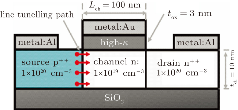
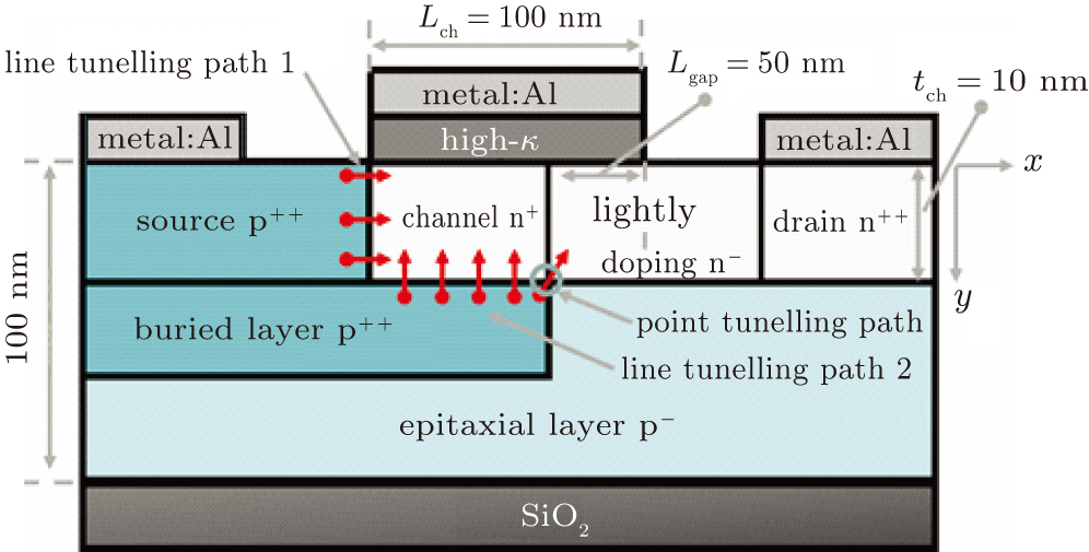
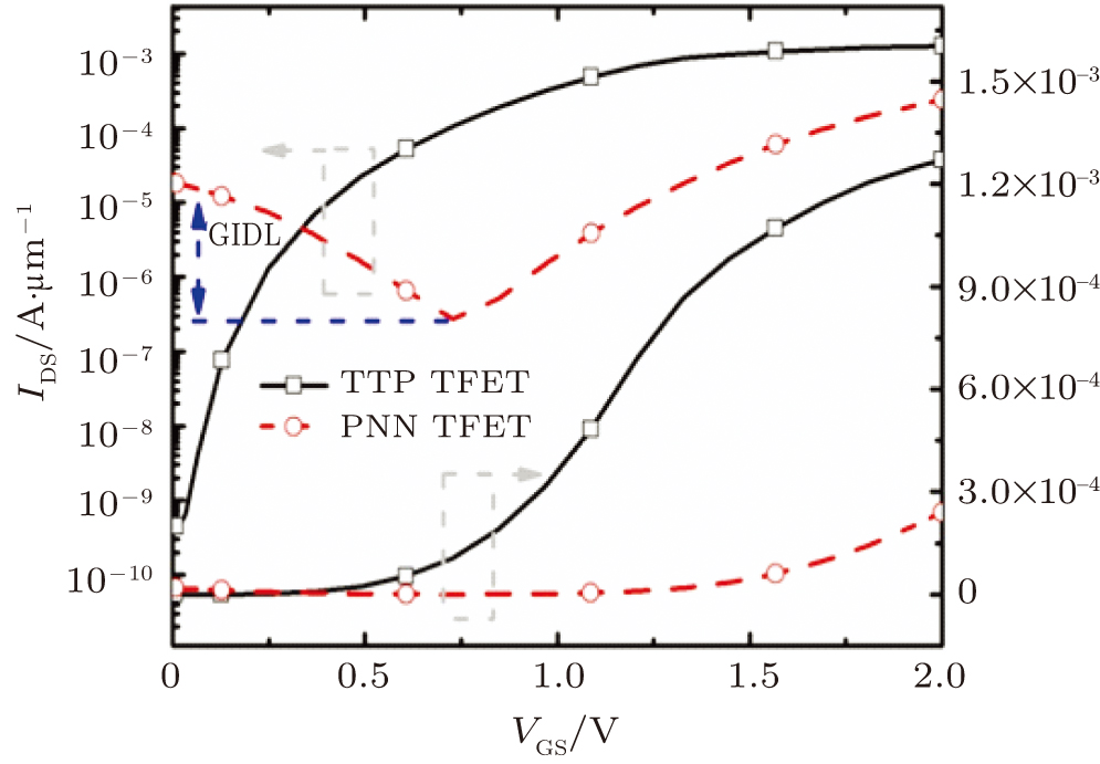
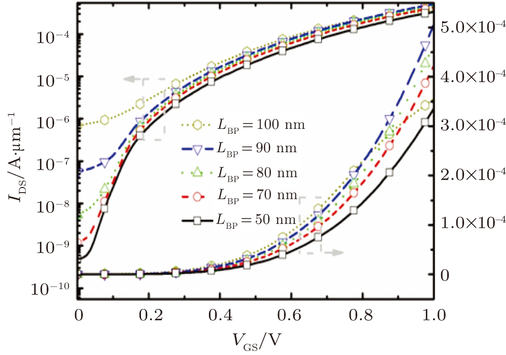
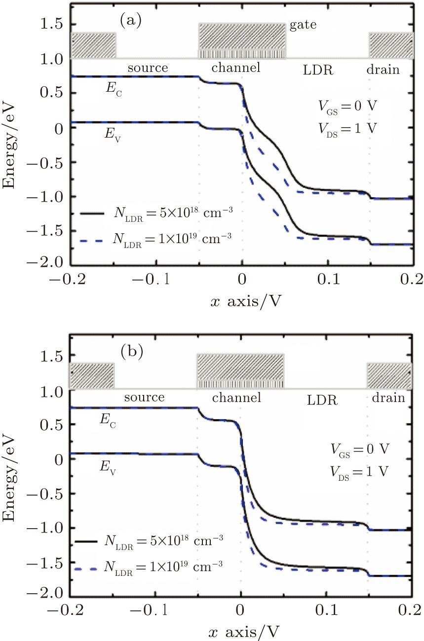
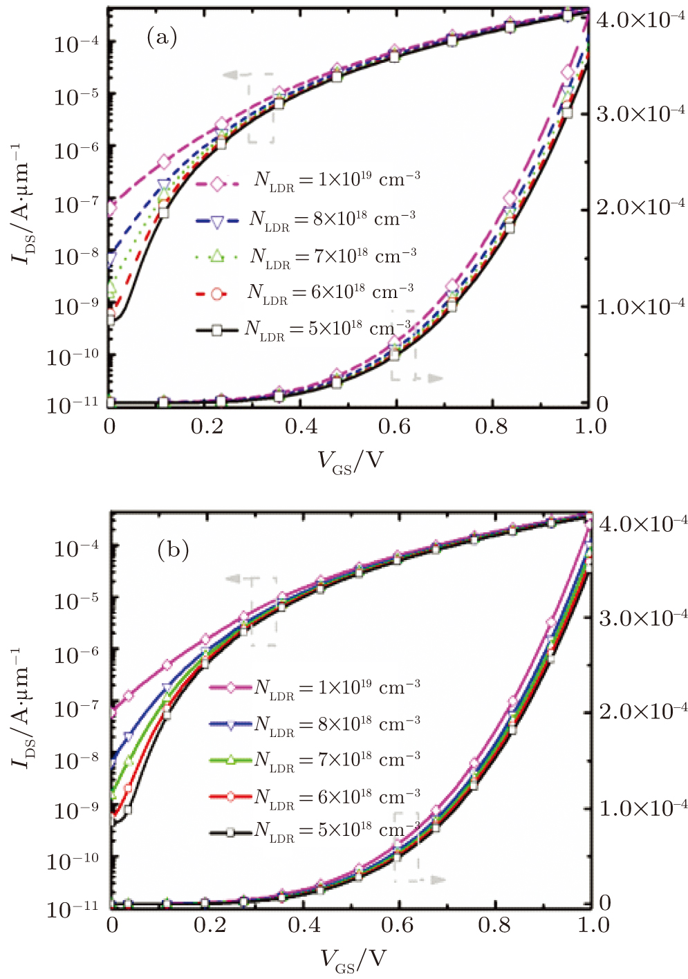
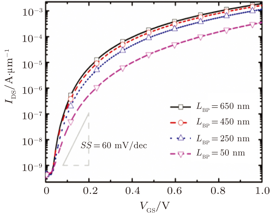
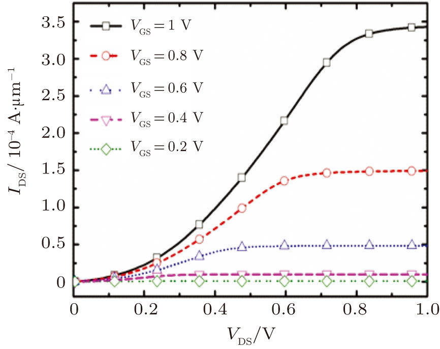
Abstract Large threshold voltage and small on-state current are the main limitations of the normal tunneling field effect transistor (TFET). In this paper, a novel TFET with gate-controlled P+N+N+ structure based on partially depleted GeOI (PD-GeOI) substrate is proposed. With the buried P+-doped layer (BP layer) introduced under P+N+N+ structure, the proposed device behaves as a two-tunneling line device and can be shut off by the BP junction, resulting in a high on-state current and low threshold voltage. Simulation results show that the on-state current density Ion of the proposed TFET can be as large as 3.4 × 10⁻⁴ A/μm, and the average subthreshold swing (SS) is 55 mV/decade. Moreover, both of Ion and SS can be optimized by lengthening channel and buried P+ layer. The off-state current density of TTP TFET is 4.4 × 10⁻¹⁰ A/μm, and the threshold voltage is 0.13 V, showing better performance than normal germanium-based TFET. Furthermore, the physics and device design of this novel structure are explored in detail.
|
Received: 23 April 2020
Revised: 26 May 2020
Accepted manuscript online: 05 June 2020
|
|
PACS:
|
74.55.+v
|
(Tunneling phenomena: single particle tunneling and STM)
|
| |
85.30.Tv
|
(Field effect devices)
|
| |
85.30.De
|
(Semiconductor-device characterization, design, and modeling)
|
|
|
Corresponding Authors:
†Corresponding author. E-mail: wbin@xidian.edu.cn
|
| About author: †Corresponding author. E-mail: wbin@xidian.edu.cn * Project supported by the National Natural Science Foundation of China (Grant No. 61704130), the Science Research Plan in Shaanxi Province, China (Grant No. 2018JQ6064), and the Science and Technology Project on Analog Integrated Circuit Laboratory, China (Grant No. JCKY2019210C029). |
Cite this article:
Bin Wang(王斌)†, Sheng Hu(胡晟), Yue Feng(冯越), Peng Li(李鹏), Hui-Yong Hu(胡辉勇), and Bin Shu(舒斌) Simulation study of device physics and design of GeOI TFET with PNN structure and buried layer for high performance 2020 Chin. Phys. B 29 107401
|
| [1] |
Benneventi G B, Gnani E, Gnud A, Reggianii S, Baccarani G 2015 IEEE Trans. Electron Dev. 62 44 DOI: 10.1109/TED.2014.2371071 |
| [2] |
Mallikarjunarao, Ranjan R, Pradhan K P, Artola L, Sahu P K 2016 Superlattices Micro. 97 70
|
| [3] |
|
| [4] |
Aslam M, Yadav S, Soni D, Sharma D 2017 Superlattices Micro. 112 86
|
| [5] |
|
| [6] |
|
| [7] |
|
| [8] |
Soni D, Sharma D, Yadav S, Aslam M, Sharma N 2018 Superlattices Micro. 113 94
|
| [9] |
|
| [10] |
|
| [11] |
Wang W, Wang P F, Zhang C M, Lin X, Liu X Y, Sun Q Q, Zhou P, Zhang D W 2014 IEEE Trans. Electron Dev. 61 193 DOI: 10.1109/TED.2013.2289075 |
| [12] |
|
| [13] |
|
| [14] |
|
| [15] |
Singh B, Rai T, Gola D, Singh K, Goel E, Kumar S, Tiwari P, Jit S 2017 Materials Science in Semiconductor Processing 71 161 DOI: 10.1016/j.mssp.2017.07.014 |
| [16] |
Low K, Zhan C, Han G, Yang Y, Goh K, Guo P, Toh E, Yeo Y 2012 Jpn. J. Appl. Phys. 51 02
|
| [17] |
Mitra S, Goswami R, Bhowmick B 2016 Superlattices Micro. 92 37
|
| [18] |
|
| [19] |
|
| [20] |
|
| [21] |
Avci U, Chu-Kung B, Agrawal A, Dewey G, Le V 2015 IEEE International Electron. Dev. Meeting December 7–9, 2015 Washington DC, USA 891
|
| [22] |
Krishnamohan T, Kim D, Raghunathan S, Saraswat K 2008 IEEE International Electron. Dev. Meeting December 15–17, 2008 San Francisco, USA
|
| [23] |
Zhang Q, Sutar S, Kosel T, Seabaugh A 2009 Solid-State Electrons 53 30
|
| [24] |
Takagi S, Kim W, Jo K, Matsumura R, Takaguchi R, Katoh T, Bae T, Kato K, Takenaka M 2018 ECS Trans. 86 75
|
| [25] |
Katoh T, Matsumura R, Takaguchi R, Takenaka M, Takagi S 2018 Jpn. J. Appl. Phys. 57 04
|
| [26] |
Matsumura R, Katoh T, Takaguchi R, Takenaka M, Takagi S 2018 Jpn. J. Appl. Phys. 57 04
|
| [27] |
Liu X, Hu H Y, Wang B, Wang M, Han G, Cui S, Zhang H M 2017 Superlattices Micro. 102 7
|
| [28] |
|
| [29] |
Colinge J P, Lee C W, Afzalian A, Akhavan N, Yan R, Ferain I, Razavi P, O’Neil B, Blake A, White M, Kelleher A, McCarthy B, Murphy R 2010 Nat. Nanotechnol. 5 225 DOI: 10.1038/nnano.2010.15 |
| No Suggested Reading articles found! |
|
|
Viewed |
|
|
|
Full text
|
|
|
|
|
Abstract
|
|
|
|
|
Cited |
|
|
|
|
Altmetric
|
|
blogs
Facebook pages
Wikipedia page
Google+ users
|
Online attention
Altmetric calculates a score based on the online attention an article receives. Each coloured thread in the circle represents a different type of online attention. The number in the centre is the Altmetric score. Social media and mainstream news media are the main sources that calculate the score. Reference managers such as Mendeley are also tracked but do not contribute to the score. Older articles often score higher because they have had more time to get noticed. To account for this, Altmetric has included the context data for other articles of a similar age.
View more on Altmetrics
|
|
|