Effect of cryogenic temperature characteristics on 0.18-μm silicon-on-insulator devices
Xie Bingqing, Li Bo, Bi Jinshun, Bu Jianhui, Wu Chi, Li Binhong, Han Zhengsheng, Luo Jiajun†,
Key Laboratory of Silicon Device and Technology, Institute of Microelectronics, Chinese Academy of Sciences, Beijing 100029, China


† Corresponding author. E-mail: luojj@ime.ac.cn

Project supported by the National Natural Science Foundation of China (Grant Nos. 61176095 and 61404169) and the Youth Innovation Promotion Association of Chinese Academy of Sciences.

Abstract
Abstract

The experimental results of the cryogenic temperature characteristics on 0.18-μm silicon-on-insulator (SOI) metal-oxide-silicon (MOS) field-effect-transistors (FETs) were presented in detail. The current and capacitance characteristics for different operating conditions ranging from 300 K to 10 K were discussed. SOI MOSFETs at cryogenic temperature exhibit improved performance, as expected. Nevertheless, operation at cryogenic temperature also demonstrates abnormal behaviors, such as the impurity freeze-out and series resistance effects. In this paper, the critical parameters of the devices were extracted with a specific method from 300 K to 10 K. Accordingly, some temperature-dependent-parameter models were created to improve fitting precision at cryogenic temperature.

1. Introduction

Nowadays, cryogenic integrated circuits have aroused great interest as a result of the high enthusiasm for Lunar and Martian exploration. However, the reliability of semiconductor devices to cryogenic environment confront more serious issues. The surprisingly extreme temperature of space background as low as 3 K makes the operation of electronics system quite difficult.[1,2] Presently, spacecraft operating in the cryogenic environment of deep space carries on-board radioisotope heating units to maintain a safe operating temperature for the electronic system.[3] This is not an ideal solution since the required active thermal control system increases cost and complexity. Meanwhile, some indispensable sub-systems such as high-sensitivity cooled sensors are required to operate in cryogenic environment. Particularly, sensors in SOI MOS process show an excellent cryogenic performance compared with bulk MOS process.[4] Hence, devices capable of operation at cryogenic temperatures will not only tolerate the unamiable space environment, but also reduce the weight of craft.

The SOI MOS offers several benefits over bulk MOS technology, such as latch-up immunity, especially in the space application due to its excellent radiation hardness.[57] The long-recognized advantages of MOS working at cryogenic temperature have encouraged investigators in many fields all over the world since the 1970s.[8] The main advantages of MOS under cryogenic temperature are associated with an increased carrier mobility, better turn-on capabilities, higher saturation velocity, higher thermal and electrical conductivity, lower power consumption, reduced thermal noise, and decrease of junction leakage currents.[9,10] With liquid nitrogen, Jason investigated the characteristic of bulk MOS.[11] With the increasing miniaturization of microelectronic technology, the experimental results for 0.1-μm MOS were reported in 1987 for the first time.[12] Recently, the reliability of 65-nm MOS was investigated in 2015.[13] The research on SOI technology at cryogenic temperature started a little later than on bulk silicon. Young and Elewa reported the advantages of cryogenic operation of SOI MOS as far back as 1990.[14,15] For the use of sub-20-nm CMOS technology, Shin investigated the characterization of advanced FD-SOI MOS at cryogenic temperature.[16] However, some specific problems related to the cryogenic temperature, such as the impurity freeze-out and series resistance effects, make it difficult for some practical applications. So as to solve some problems, a circuit structure featured twin-gate was proved effective at very low temperature.[17] More recently, Sansen obtained an 8-bit analog-to-digital converter working from 4.2 K to 300 K, guaranteeing the reliability of circuits at cryogenic temperature.[18]

Previous work was always concentrated in the area of cryogenic IV performance of SOI MOS.[1921] In this work, the experimental results of cryogenic IV and CV performance of SOI MOSFETs with a radiation-hard architecture in a 0.18-μm process are presented. Some specific behaviors at cryogenic temperature are analyzed. More specifically, numerical models of several key parameters are described.

2. Device technology and experimental setup

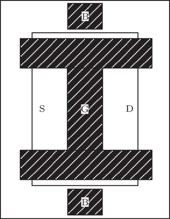
Due to the excellent performance in radiation hardness, devices with H-gate are generally used in the radiation-hard application.[22] In this paper, the devices are H-gate using 0.18 μm PDSOI process as shown in Fig. 1. The gate-oxide layer is 2.9 nm. Both the silicon-film layer and buried oxide layer are 300 nm.

Fig. 1. Structure of H-gate.

To investigate the impact of cryogenic temperature, the gate width and length of the device in our test are both 20 μm to eliminate the effects of a short channel and narrow channel. In order to decrease the effect of noise and gate resistance in CV test, a multiple fingers gate is utilized. In IV test we investigated MOSFETs with gate length (L) and width (W) both of 20 μm. In CV test, the MOSFET of which L and W are 10 μm and 100 μm respectively has 20 fingers. As shown in Fig. 2, a low-temperature probe system which can enable on-chip testing from 300 K to 6 K is used in the experiment. The devices were placed on a copper pallet cooled by liquid helium. The parameters of devices can be measured by the Keithley 4200 semiconductor characterization system.

Fig. 2. Experimental setup for cryogenic measurements.
3. Experiments and results
3.1. IV performance

The output characteristics of the NMOSFET (W = 20 μm, L = 20 μm) from room temperature to cryogenic temperature can be seen in Fig. 3(a). We can plot the saturation drain current IDsat derived from the saturation region, as can be seen in Fig. 3(b), and saturation drain current increases by a factor of approximately 3 when cooled to 10 K. The resistance in linear region Rlinear varying with temperature can be derived from the linear region as shown in Fig. 3(c). Both IDsat and Rlinear curves change sharply within the temperature interval from 300 K to 40 K and are flat below 40 K.

Fig. 3. (a) Drain current versus VDS; (b) saturation drain current versus temperature; (c) linear resistance versus temperature, from 300 K to 10 K.

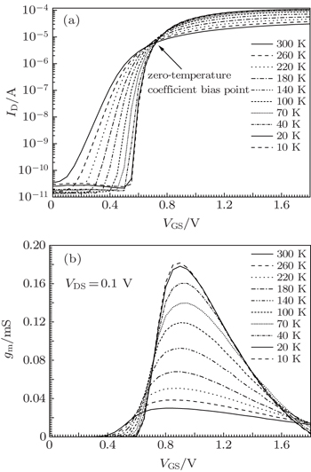
Figures 4(a) and 4(b) show the transfer curves and transconductance varying with temperature respectively. In Fig. 4(a), we can see that the characteristics have a zero-temperature coefficient (ZTC) point in which the circuits can be stable from room temperature to cryogenic temperature.[23] This point is useful in the design of a high-precision amplifier. In consideration of IC design, transconductance (gm) is very important in that it can be used to show the ability of converting voltage (V) to obvious current (I). At the same time, gm is a primary parameter in that it is a design guideline for analog design, and gm can be expressed as

The maximum of transconductance is about 30 μS at 300 K and the value increases to nearly 180 μS at 10 K, which is induced by the increase of mobility at cryogenic temperature.

Fig. 4. (a) Drain current versus gate-to-source voltage; (b) transconductance versus gate-to-source, from 300 K to 10 K.

The sub-threshold swing S is defined as

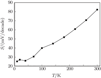
where k, T, and q denote Boltzmann’s constant, Kelvin temperature, and electron charge, respectively, and n is a factor mainly associated with the capacitance derived from the traps near the interface and gate-to-oxide capacitance COX.[21] Note that in Eq. (2), S is proportional to temperature at certain n (n ≃ 1.4 in our test). The sub-threshold swing at 300 K is approximately 70 mV/decade to 110 mV/decade.[19] As shown in Fig. 5 at 10 K, the sub-threshold swing is reduced almost 3.3 times, which means a smaller power supply can be utilized. Meanwhile when temperature is below nearby 40 K, S is no longer proportional to temperature which may be induced by the factor n derived from change of capacitance in cryogenic environment.

Fig. 5. Sub-threshold swing versus temperature, from 300 K to 10 K.
3.2. CV performance

It is very important to maintain the reliability of COX. The CV characteristic is universally used to measure some important parameters such as the thickness of oxide, Vth, and flatband voltage. In this paper, characterization analysis of MOS capacitors will be carried out at a high frequency of 1 MHz. The CV test strategy in Keithley 4200 is implemented by applying a small alternating voltage to the MOSFET under test. Q can be derived by integrating the current over time, and C can be calculated from

To get the characteristic of gate-to-bulk capacitance CGB, the nodes gate and bulk of SOI NMOSFET are connected to the semiconductor characterization system, and the node drain and source are opened. The experimental result of CGB versus temperature is shown in Fig. 6(a). As can be seen, the capacitance varies with temperature in the accumulation region that CGB increases with decreasing temperature. The characteristics of oxide layer SiO2 are considered as almost invariable with temperature. CGB here cannot be recognized as COX due to the influence of series resistance. The capacitance CGD and CGB were also tested, and the result shows that CGS is equal to CGD due to the symmetrical architecture in our devices. Figure 6(b) illustrates the characteristics of CGDVGD varying with temperature.

Fig. 6. (a) CGBV; (b) CGDV versus temperature (from 300 K to 10 K).

Starting from about 20 K, a specific behavior was observed and the CGB curves do not coincide with each other at adjacent measurement cycles and finally converge to a certain curve after some test iterations, and the same phenomenon exists in CGB curve of PMOSFET, as shown in Fig. 7. The phenomenon only occurs when the interval between adjacent measurement cycles is short enough, an explanation is the charging and recharging of traps.[24]

Fig. 7. Drifting of CGB curve (NMOSFET) in cryogenic temperature.
4. Discussion
4.1. Series resistance at cryogenic temperature

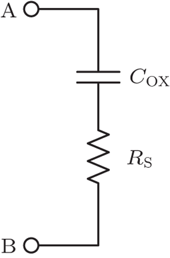
The COX is commonly defined as the capacitance in a strong accumulation region. However, the series resistance Rs is unavoidable in the device of a semiconducting film on a nonconducting substrate. Series resistances in our test mainly arise from the undepleted region between the tunnel and the body tie. To measure series resistance, the simple circuit can be utilized to analyze, as shown in Fig. 8.

Fig. 8. Simplified model used to determine RS in accumulation region.

The equal capacitance Cm and conductance Gm can be tested by semiconductor characterization system. The admittance Ym across terminals A–B (see Fig. 8) in a strong accumulation region can be calculated by[25]

where j is the unit of imaginary part, and ω is the angular frequency. The series resistance can be derived from Eq. (4) as

The measured oxide capacitance COXm is given by

It is shown that COXm is smaller than the theoretical value of COX due to Rs. The corrected capacitance Cadj and corrected conductance Gadj at the frequency of interest are calculated by

and

respectively, where . As shown in Fig. 9(a), Cadj has obvious distinctions with measured capacitance. COXm derived from Fig. 6(a) and corrected oxide capacitance COXadj derived from Fig. 9(a) are given in Fig. 9(b). The variation of series resistance with temperature can be seen in Fig. 9(c). The Rs has a huge influence on the measurement of oxide capacitance. COXadj is nearly constant or increases slightly with temperature, which is understandable for the dielectric constant almost invariant at cryogenic temperature. Because of the increase of effective mobility, Rs is reduced by about 40% as temperature decreases from 300 K to 10 K, and that curve is almost flat below 100 K because the surface roughness depresses the increase of mobility. The numerical model of Rs from 300 K to 10 K is

where Rs0 is the series resistance at 300 K and J1 is the corrected constant.

Fig. 9. (a) Corrected CV curve versus temperature; (b) measured oxide capacitance COXm and corrected oxide capacitance COXadj; (c) calculated series resistance Rs versus temperature, from 300 K to 10 K.
4.2. Flatband voltage influenced by freeze-out effect at cryogenic temperature

Flatband voltage represents an important parameter that can be derived from flatband capacitance CFB. As is well known, CFB is calculated as[11]

where A is the gate area, ɛsi is the permittivity of silicon substrate, and LD is the extrinsic Debye length defined as

However, equation (10) is under the hypothesis that impurity has been completely ionized, which means the doping NA is assumed constant. It is not compatible with the cryogenic operation due to freeze-out effect. The CFB at cryogenic temperature can be given by[27]

where ρs is the charge density at surface, ψs and ψb are Fermi energies at surface and band, respectively. Considering

where n and p respectively denote concentrations of electrons and holes, and denote the concentration of ionized acceptor and donor, respectively.[28]

where Ec and Ev, respectively, denote the conduction and valence band, Nc and Nv are the corresponding effective density of states, gd and ga denote degeneracy factors of donors and acceptors, and F1/2 denotes Fermi–Dirac operator of one-half order. The relation between various terms of Eqs. (14)–(17) may be determined by

and

where mp and mn is the effective mass of hole and electron, respectively, EG denotes temperature-dependent energy gap, and ΔEA denotes ionization energies of the impurities.[29]

The Fermi–Dirac statistics is necessary for at cryogenic temperature, because the Fermi level EF is higher than the acceptor level EA when temperature is under 70 K in our calculation. As shown in Fig. 10, the concentration of ionized acceptor decreases obviously when temperature is below 70 K. However, in p-type semiconductor as Fermi level approaches the valance band, it will still remain several kT (about 6 kT in our calculation) below the top of the valance band, as discussed by Mckelvey.[30] Therefore, the Boltzmann approximation can be utilized to the holes in the valence band. For the sake of completeness, CFB can be derived as

Fig. 10. Concentration of ionized acceptor versus temperature.
4.3. Threshold voltage at cryogenic temperature

As is well known, Vth is defined as the gate voltage when the surface potential Ψs is equal to 2ΨB, where ΨB is the Fermi potential of bulk. In this paper, threshold voltage is determined from the device turn-on characteristic in the linear region. For NMOSFET, threshold voltage is defined as

where VFB is the flatband voltage.[24] The Fermi potential is increased when the temperature decreases. As a result, Vth is increased as shown in Fig. 11, and the rise amplitude can be 40% as temperature is reduced from room temperature to 10 K. What should be noticed is that the Vth is nearly constant below 70 K. The variation of slope is determined by the carrier freeze-out below freeze-out temperature (nearby 70 K). In the range from 300 K to 70 K, we can get the numerical model of threshold voltage as

where Vth0 is the threshold voltage at 300 K, Vth is linear as temperature decreases from room temperature to 70 K, and K1 is corrected constant.

Fig. 11. Measured threshold voltage and fitting curve, from 300 K to 10 K.

Furthermore in Eq. (26), VFB and ΨB are affected by temperature. The bulk potential ΨB can be calculated as

where ni is the intrinsic carrier concentration defined as

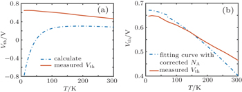
Using corrected , the VFB suiting for cryogenic temperature is derived from corrected capacitance (Fig. 9(a)). However, a problem is proposed in solving Eq. (25) numerically. For simplicity, we make use of the assumptions: i) concentration of acceptor is completely ionized from 300 K to 70 K; ii) at 50 K delegates the concentration of ionized acceptor below 70 K (see Fig. 10). The corrected Vth is shown in Fig. 12(b). As a result, the corrected Vth confirms the validity of this model.

Fig. 12. Calculated and measured Vth, from 300 K to 10 K (a) with complete ionization of NA; (b) with corrected .
5. Conclusion

The cryogenic characteristics of H-gate SOI MOS fabricated with 0.18-μm PDSOI process are presented in this paper. Both of the important IV and CV parameter variations with temperature from 300 K to 10 K are discussed. We observe an obvious decrease in sub-threshold swing S and increase in transconductance Gm at cryogenic temperature. As temperature decreases, the decrease of series resistance exerts a huge impact on the test of oxide capacitance due to higher effective carrier mobility.

The freeze-out effect should be considered at cryogenic temperature, because it can reduce the concentration of ionized impurities which have a big influence on electrical parameters. For example, it can induce the Fermi-energy drift and narrow the energy gap, thus increasing the magnitude of flatband voltage and further increasing threshold voltage Vth. As a result, the current of MOS will be changed.

Furthermore, the comparison of different structures (traditional straight-gate and H-gate) will be done in later work. The significant IV and CV performance of SOI MOSFETs at cryogenic temperature provides an immense potential in the deep space application.

Reference
1Elbuluk MHammoud APatterson R2005IEEE 36th Power Electronics Specialists ConferenceJune 16, 2005USA1156
2Chen TZhu CNajafizadeh LJun ongimAhmed dnanDiestelhorst yanEspinel GCressler J D 2006 Solid-State Electron. 50 959
3Venkataraman SBanerjee BChang-Ho LLaskar JCressler J D2008Topical Meeting on Silicon Monolithic Integrated Circuits in RF SystemsJan 10–12, 2007Long Beach, USA52
4Wada TNagata HIkeda HArai YOhno MNagase K 2012 Journal of Low Temperature Physics 167 602
5Zhao XMei BBi J SZheng Z SGao L CZeng C BLuo J JYu FHan Z S 2015 Acta Phys. Sin. 64 294 (in Chinese)
6Lu KChen JLuo J XHe W WHuang J QChai ZWang X 2015 Chin. Phys. 24 088501
7Zhou HCui J WZheng Q WGuo QRen D YYu X F2015Acta Phys. Sin.64086101(in Chinese)
8Gaensslen FRideout VWalker EWalker J 1977 IEEE Electron Dev. 24 218
9Ghibaudo GBalestra F 1996 Journal de Physics IV 6 C3-3
10Clark W FEl-Kareh BPires R GTitcomb S LAnderson R L 1992 IEEE T. Compon. Hybr. 15 197
11Jason WJames P 1986 IEEE Electron Dev. 33 1012
12Sai-Halasz GWordeman MKern PGanin ERishton SZicherman DSchmid HPolcari RNg HRestle PChang TDennard R 1987 IEEE Electron Dev. Lett. 8 563
13Hoff JDeptuch GWu G YGui P 2015 IEEE T. Nucl. Sci. 62 1255
14Young KTsaur Y 1990 IEEE Electron Dev. Lett. 11 126
15Elewa TBalestra FCristoloveanu SHafez MColinge JAuberton-Herve JDavis R 1990 IEEE Electron Dev. 37 1007
16Shin MShi MMouis MCros AJosse EKim TGhibaudo G201415th International Conference on Ultimate Integration on Silicon (Ulis)61
17Claeys CSimoen E 1994 Electron. Lett. 30 454
18Creten YMerken PSansen WMertens PVan Hoof C 2009 IEEE J. Solid-St. Circ. 44 2019
19Seung-Ho HGil-Bok CRock-Hyun BHee-Sung KSung-Woo JYoon-Ha J 2008 IEEE Electron Dev. Lett. 29 775
20Das KLehmann T 2014 Cryogenics 62 84
21de Souza MPavanello AMartino ASimoen EClaeys C2007IEEE International Soi Conference Proceedings3710.1109/SOI.2007.4357844
22Damiano JFranzon P D2004IEEE International SOI ConferenceOct. 4–7, 2004Charleston, USA115
23Prijie Z DDimitrijev S SStojadinovie N D 1992 Microelectronics Reliability 32 769
24Das KLehmann T2010IEEE International Symposium on Circuits and Systems (ISCAS)May 30–June 2, 2010Paris, France3405
25Nicollian E HBrews J R1982MOS (Metal Oxide Semiconductor) Physics and TechnologyNew YorkWiley224227224–7
26Sze S MKwok K2006Physics of Semiconductor Devices2nd edn.New YorkWiley374413374–413
27Ghazavi PFat D H 1995 IEEE Electron Dev. Lett. 42 123
28Cheng-Linag HGildenblat G S 1989 IEEE Electron Dev. Lett. 36 1434
29Gaensslen F HJaeger R C 1979 Solid-State Electronics 22 423
30McKelvey Solid State and Semiconductor PhysicsNew YorkDoverch. 910.1007/978-3-642-36748-9_16