| INTERDISCIPLINARY PHYSICS AND RELATED AREAS OF SCIENCE AND TECHNOLOGY |
Prev
Next
|
|
|
Design and investigation of dopingless double-gate line tunneling transistor: Analog performance, linearity, and harmonic distortion analysis |
| Hui-Fang Xu(许会芳)†, Xin-Feng Han(韩新风), and Wen Sun(孙雯) |
| 1 Institute of Electrical and Electronic Engineering, Anhui Science and Technology University, Fengyang 233100, China |
|
|
|
|
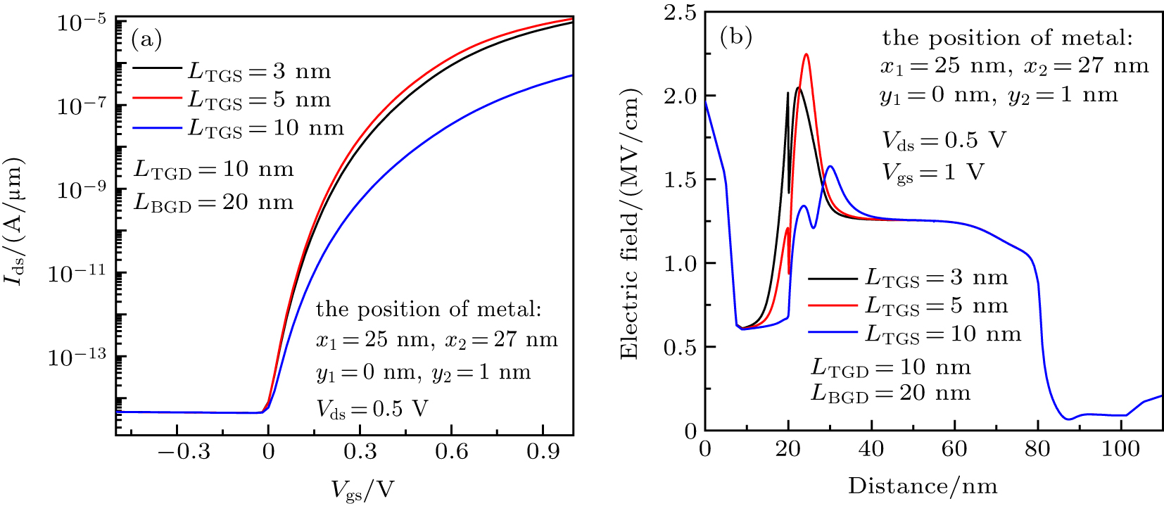
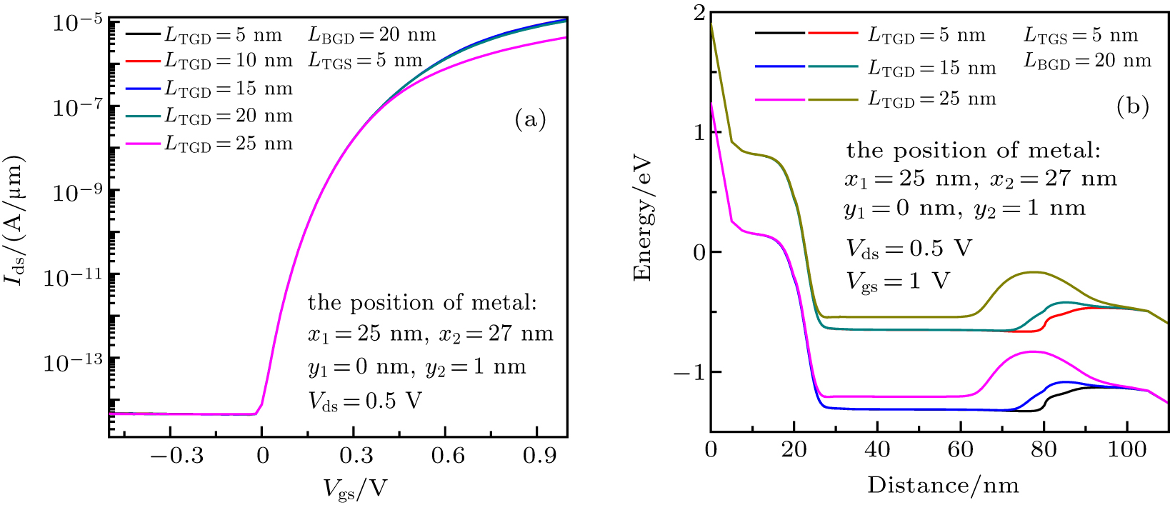
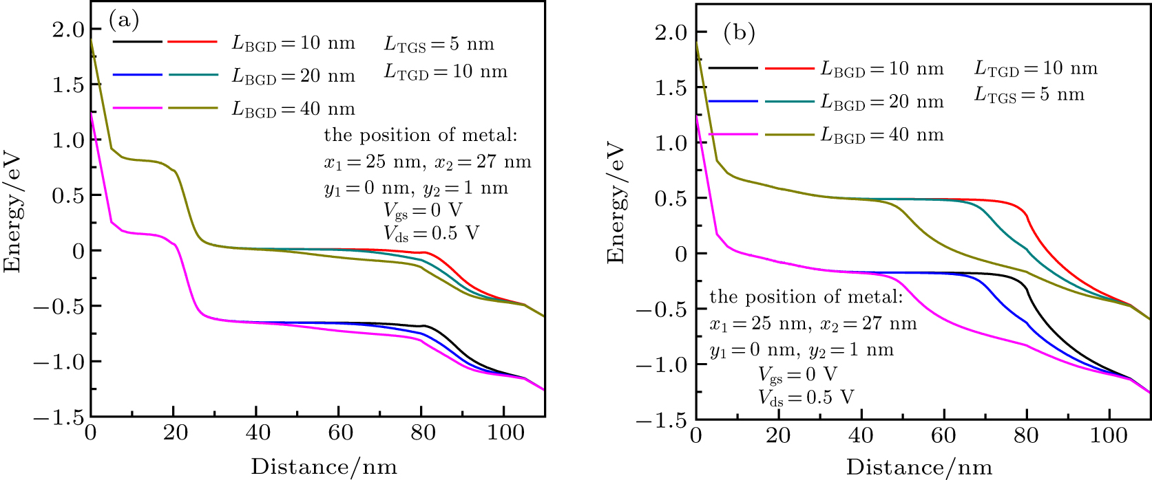
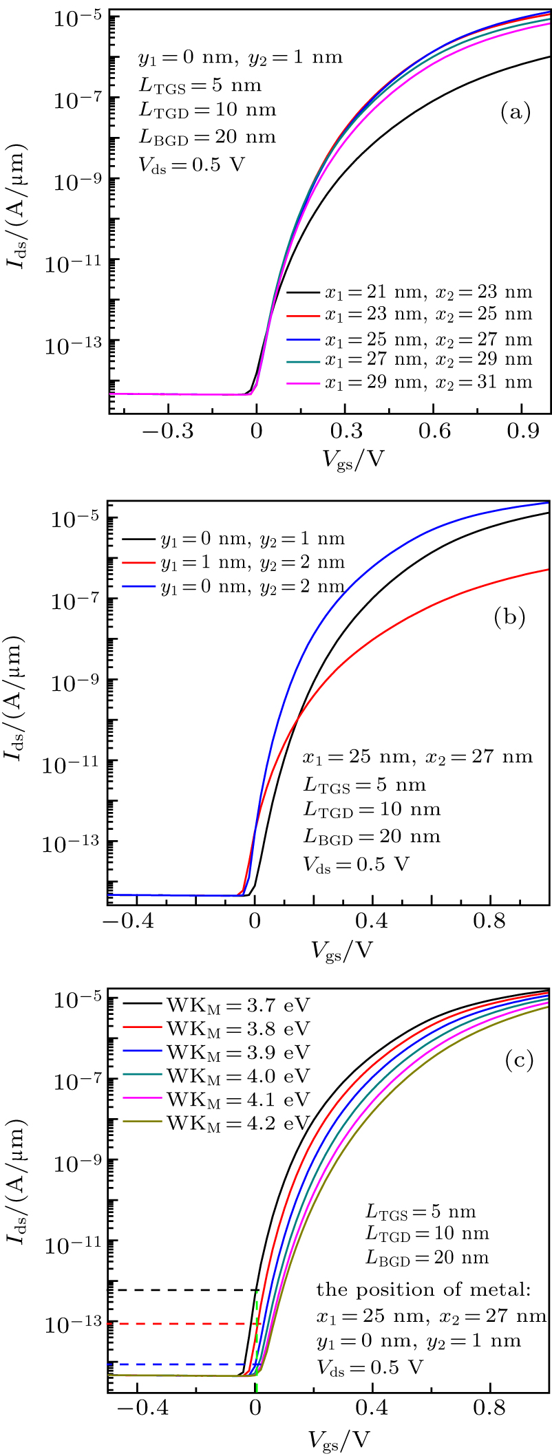
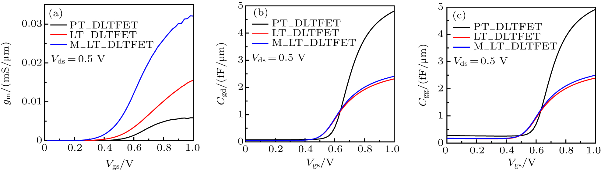
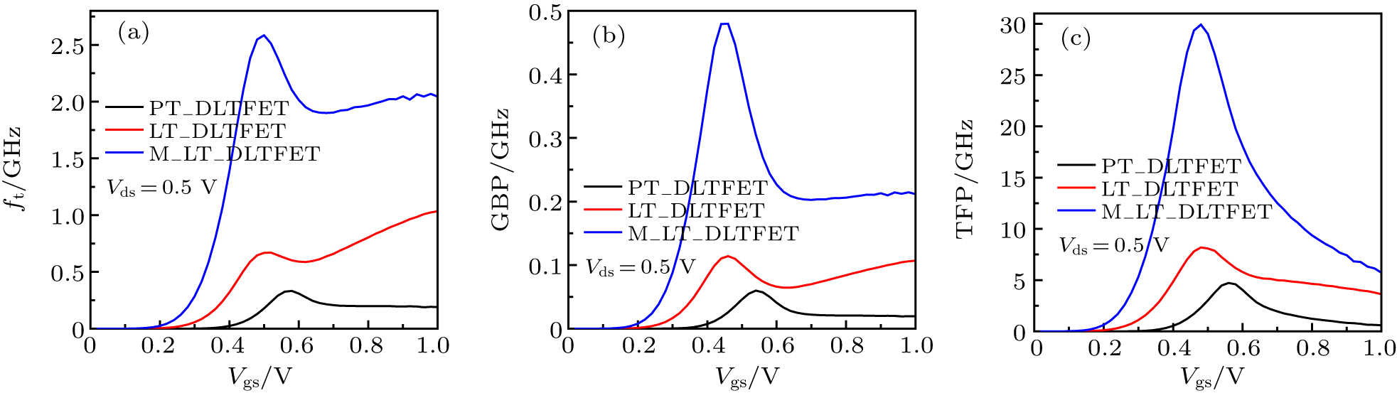
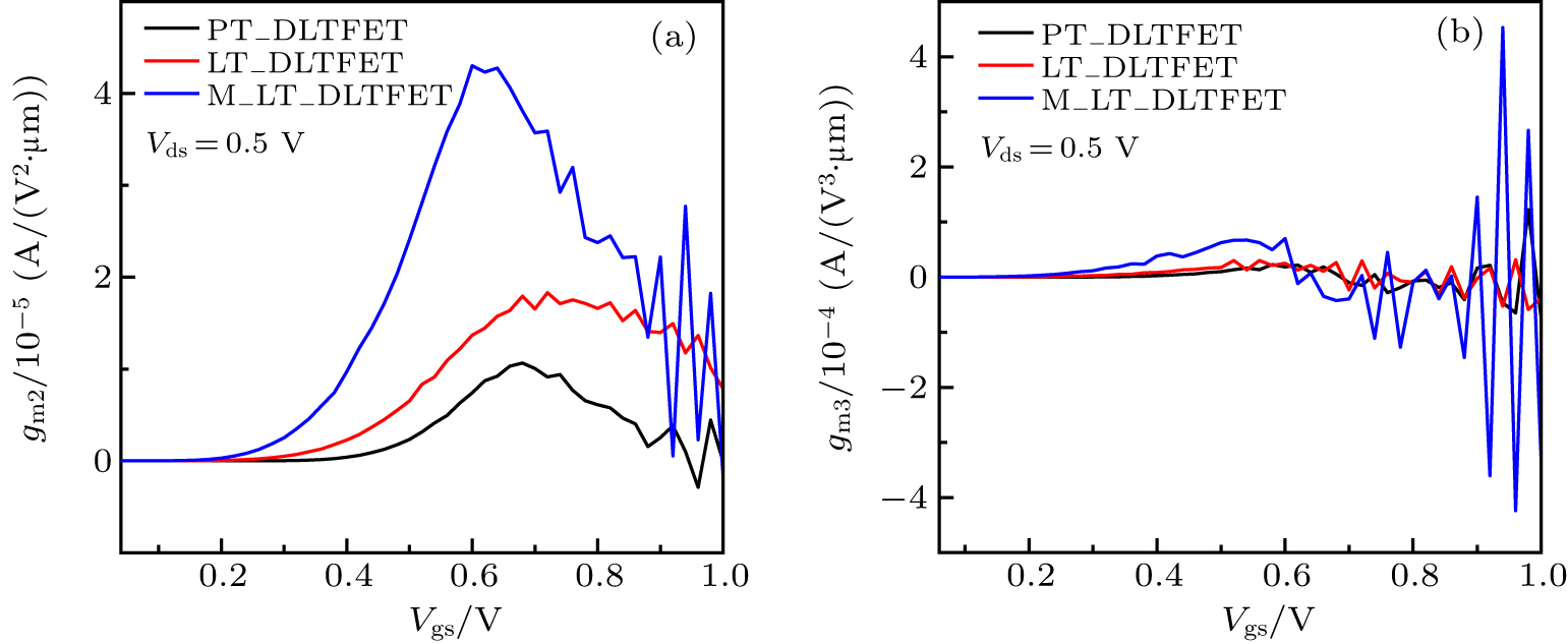
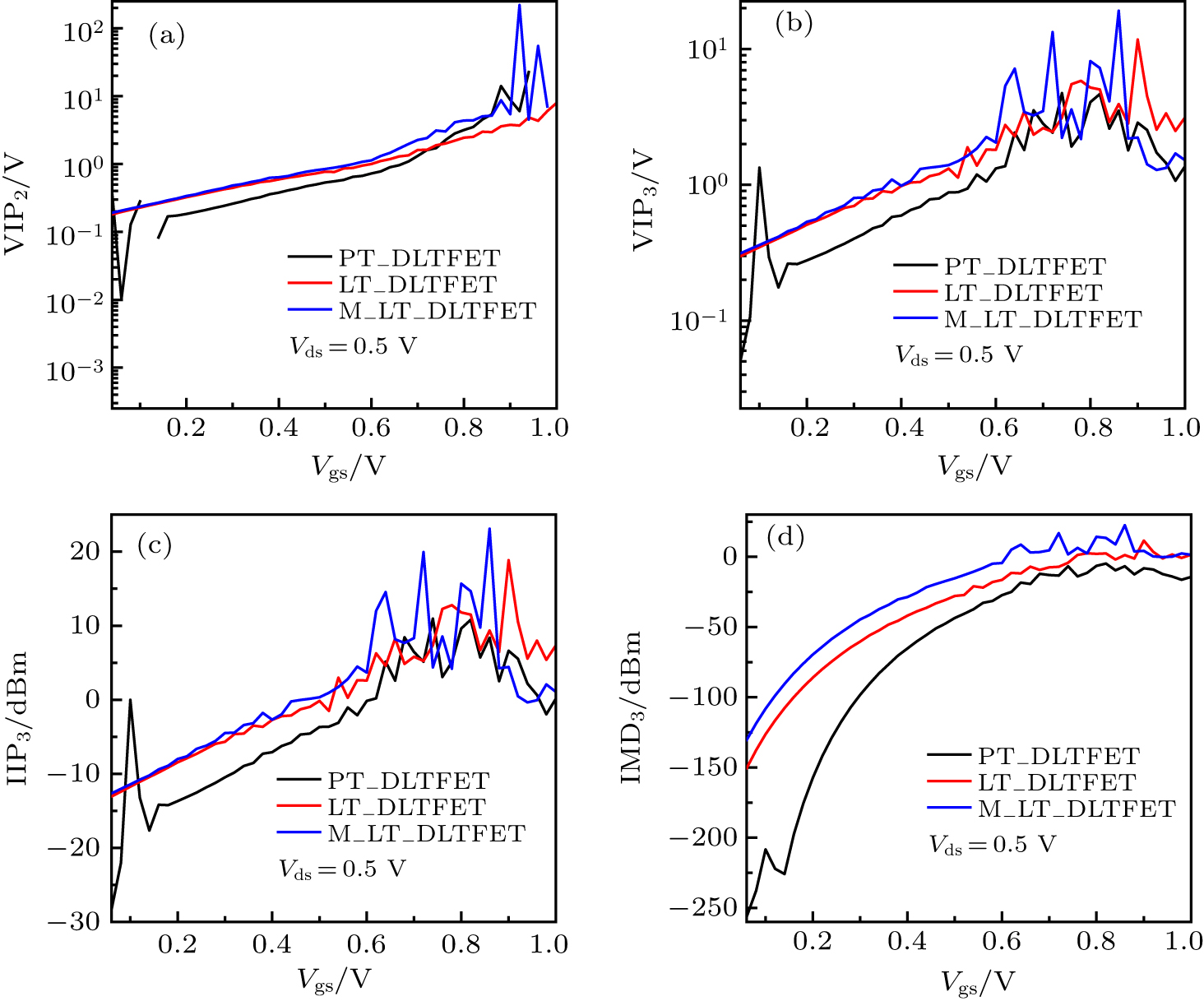
Abstract The tunnel field-effect transistor (TFET) is proposed by using the advantages of dopingless and line-tunneling technology. The line tunneling is created due to the fact that the gate electric field is aligned with the tunneling direction, which dramatically enhances tunneling area and tunneling current. Moreover, the effects of the structure parameters such as the length between top gate and source electrode, the length between top gate and drain electrode, the distance between bottom gate and drain electrode, and the metal position on the on-state current, electric field and energy band are investigated and optimized. In addition, analog/radio-frequency performance and linearity characteristics are studied. All results demonstrate that the proposed device not only enhances the on/of current ratio and reduces the subthreshold swing, but also offers eight times improvement in cut-off frequency and gain band product as compared with the conventional point tunneling dopingless TFET, at the same time; it shows better linearity and small distortions. This proposed device greatly enhances the potential of applications in dopingless TFET.
|
Received: 13 April 2020
Revised: 20 May 2020
Accepted manuscript online: 12 June 2020
|
|
PACS:
|
85.30.Mn
|
(Junction breakdown and tunneling devices (including resonance tunneling devices))
|
| |
81.05.Ea
|
(III-V semiconductors)
|
| |
85.30.Tv
|
(Field effect devices)
|
|
|
Corresponding Authors:
†Corresponding author. E-mail: xu0342@163.com
|
| About author: †Corresponding author. E-mail: xu0342@163.com * Project supported by the Natural Science Research Key Project of Universities of Anhui Province, China (Grant No. KJ2017A502), the Introduced Talent Project of Anhui Science and Technology University, China (Grant No. DQYJ201603), and the Excellent Talents Supported Project of Colleges and Universities, China (Grant No. gxyq2018048). |
Cite this article:
Hui-Fang Xu(许会芳)†, Xin-Feng Han(韩新风), and Wen Sun(孙雯) Design and investigation of dopingless double-gate line tunneling transistor: Analog performance, linearity, and harmonic distortion analysis 2020 Chin. Phys. B 29 108502
|
| [1] |
|
| [2] |
|
| [3] |
|
| [4] |
|
| [5] |
|
| [6] |
Ameen T A, Ilatikhameneh H, Fay P, Seabaugh A, Rahman R, Klimeck G 2019 IEEE Trans. Electron Dev. 66 736 DOI: 10.1109/TED.2018.2877753 |
| [7] |
Sanjay K, Kunal S, Sweta C, Ekta G, Prince K S, Kamalaksha B, Balraj S, Satyabrata J 2018 IEEE Trans. Electron Dev. 65 331 DOI: 10.1109/TED.2017.2773560 |
| [8] |
|
| [9] |
|
| [10] |
|
| [11] |
|
| [12] |
|
| [13] |
|
| [14] |
|
| [15] |
|
| [16] |
|
| [17] |
|
| [18] |
|
| [19] |
|
| [20] |
|
| [21] |
|
| [22] |
Liu H, Yang L A, Jin Z, Hao Y 2019 IEEE Trans. Electron Dev. 66 3229 DOI: 10.1109/TED.16 |
| [23] |
Apoorva, Kumar N, Amin S I, Anand S 2020 IEEE Trans. Electron Dev. 67 789 DOI: 10.1109/TED.16 |
| [24] |
Naveen K, Ashish R 2019 IEEE Trans. Electron Dev. 66 4453 DOI: 10.1109/TED.16 |
| [25] |
Lin J T, Wang T C, Lee W H, Yeh C T, Glass S, Zhao Q T 2018 IEEE Trans. Electron Dev. 65 769 DOI: 10.1109/TED.16 |
| [26] |
|
| [27] |
Gaurav M, Shubham S, Raghvendra S S, Mamidala J K 2019 IEEE Trans. Electron Dev. 66 4425 DOI: 10.1109/TED.16 |
| [28] |
Ehteshamuddin M, Loan S A, Alharbi A G, Alamoud A M, Rafat M 2019 IEEE Trans. Electron Dev. 66 4638 DOI: 10.1109/TED.16 |
| [29] |
Tripuresh J, Yashvir S, Balraj S 2020 IEEE Trans. Electron Dev. 67 1873 DOI: 10.1109/TED.16 |
| [30] |
|
| [31] |
Li W, Liu H X, Wang S L, Chen S P, Han T, Yang K 2019 AIP Adv. 9 045109 DOI: 10.1063/1.5087879 |
| [32] |
ATLAS User’s Manual Silvaco Int. Santa Clara, CA 2012
|
| [33] |
Wu C L, Huang Q Q, Zhao Y, Wang J X, Wang Y Y, Huang R 2016 IEEE Trans. Electron Dev. 63 5072 DOI: 10.1109/TED.2016.2619694 |
| No Suggested Reading articles found! |
|
|
Viewed |
|
|
|
Full text
|
|
|
|
|
Abstract
|
|
|
|
|
Cited |
|
|
|
|
Altmetric
|
|
blogs
Facebook pages
Wikipedia page
Google+ users
|
Online attention
Altmetric calculates a score based on the online attention an article receives. Each coloured thread in the circle represents a different type of online attention. The number in the centre is the Altmetric score. Social media and mainstream news media are the main sources that calculate the score. Reference managers such as Mendeley are also tracked but do not contribute to the score. Older articles often score higher because they have had more time to get noticed. To account for this, Altmetric has included the context data for other articles of a similar age.
View more on Altmetrics
|
|
|