Closed-form breakdown voltage/specific on-resistance model using charge superposition technique for vertical power double-diffused metal–oxide–semiconductor device with high-κ insulator*

Project supported by the National Natural Science Foundation of China (Grant No. 61404110) and the National Higher-education Institution General Research and Development Project, China (Grant No. 2682014CX097).

Chen Xue1, Wang Zhi-Gang1, †, Wang Xi1, B Kuo James2
School of Information Science and Technology, Southwest Jiao Tong University, Chengdu 611756, China
“National” Taiwan University, Taipei, China


† Corresponding author. E-mail: zhigangwang@swjtu.edu.cn

Project supported by the National Natural Science Foundation of China (Grant No. 61404110) and the National Higher-education Institution General Research and Development Project, China (Grant No. 2682014CX097).

Abstract

An improved vertical power double-diffused metal–oxide–semiconductor (DMOS) device with a p-region(P1) and high-κ insulator vertical double-diffusion metal–oxide–semiconductor (HKP-VDMOS) is proposed to achieve a better performance on breakdown voltage (BV)/specific on-resistance (Ron,sp) than conventional VDMOS with a high-κ insulator (CHK-VDMOS). The main mechanism is that with the introduction of the P-region, an extra electric field peak is generated in the drift region of HKP-VDMOS to enhance the breakdown voltage. Due to the assisted depletion effect of this p-region, the specific on-resistance of the device could be reduced because of the high doping density of the N-type drift region. Meanwhile, based on the superposition of the depleted charges, a closed-form model for electric field/breakdown voltage is generally derived, which is in good agreement with the simulation result within 10% of error. An HKP-VDMOS device with a breakdown voltage of 600 V, a reduced specific on-resistance of 11.5 mΩ·cm2 and a figure of merit (FOM) (BV2/Ron,sp) of 31.2 MW·cm−2 shows a substantial improvement compared with the CHK-VDMOS device.

1. Introduction

Vertical double-diffused metal–oxide–semiconductor (VDMOS) device using a high-κ (HK) insulator has been investigated for power application,[15] owing to a much higher permittivity of the HK insulator for absorbing most electric displacement lines instead of the semiconductor drift region. Therefore, it could achieve a superior trade-off relationship between breakdown voltage (BV) and specific on-resistance (Ron,sp).[610] This trade-off scenario is similar to a super junction by optimizing the drift region. An analytical model of a conventional VDMOS with the HK insulator (CHK-VDMOS) is derived to calculate the electric field and BV.[1] Based on this model, it is noted that the potential contours in the drift region are not so uniformly distributed as in a super junction. The avalanche breakdown point is yielded in the source-side drift region. Optimization of electric field in the drift region of CHK-VDMOS can further minimize Ron,sp at a maximum BV by modulating electric field flux into the HK insulator.[11]

Based on intrinsic absorption of electric displacement in the HK voltage sustained layer, an improved vertical power DMOS device with a p-region and an HK insulator (HKP-VDMOS) is proposed. Taking the superposition principle of charge conservation into account for simplification,[1315] a closed-form analytical model is built for the electric field distribution and the breakdown voltage. This model is to reveal how the extra electric field peak in the bulk of the drift region is affected by space charges.

2. Device structure

Figure 1 shows the schematic views of HKP-VDMOS and CHK-VDMOS. In CHK-VDMOS, the electric displacement flows from the drift region into the HK region in the reversed blocking state, where the drift region is totally depleted, assisted by the HK region for reducing the specific on-resistance. Two columns of the N-type pillars with different doping concentrations are used to lessen the electric field peaks at the avalanche breakdown location.[12] However, in the HKP-VDMOS device, a P-type region is introduced under the gate to further reduce the electric field. Thus, the breakdown voltage is further enhanced due to an extra electric field peak generated at the junction between the P-type region and the drift region, which is depleted by the HK dielectric region and also compensated for by the P-type region. The other electric field peak is produced at the bottom of the P-type region for redistributing the vertical electric field. Therefore, a higher breakdown voltage can be achieved with the drift region being more heavily doped. In order to verify the idea of the HKP-VDMOS, Medici simulations are carried out. The parameters used in the Medici simulations are listed in Table 1. Based on the Medici simulation results, the distribution of the electric field in the p-region is shown in Fig. 2.

Fig. 1. (color online) (a) Schematic cross section of the HKP-VDMOS with the main N2-drift region, the low doping N1 region, the P-region, and the HK-region. (b) Schematic cross section of the CHK-VDMOS. An electric field peak is produced at the bottom of the P-type region for redistributing the vertical electric field.
Fig. 2. (color online) Electric fields in vertical direction versus distance along the y axis of the HKP-VDMOS with a dielectric insulator having a relative permittivity of 200 and various p-region doping densities at location x = −1.9 μm. NA is increased from 0.5 × 1015 cm−3 to 4.5 × 1015 cm−3, the electric field peak is generated in the drift region.
Table 1.

Device parameters used in Medici simulation.

.
3. Analytical model and verification
3.1. Principle of superposition

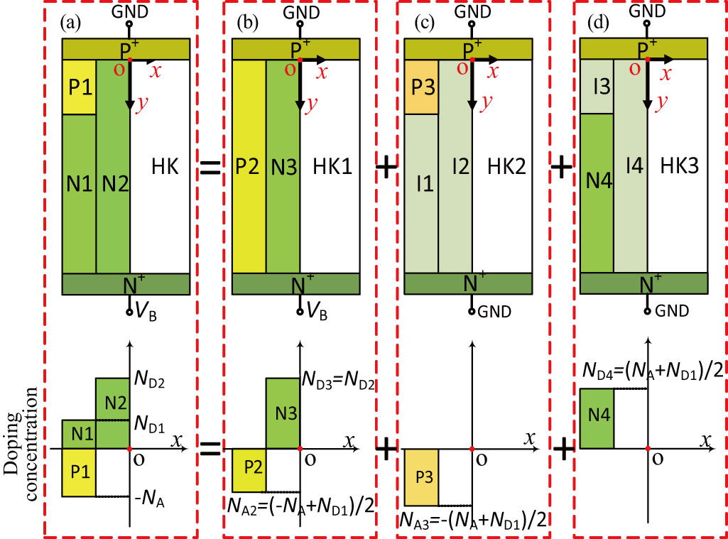
In this subsection, an analytical model of breakdown voltage/specific on-resistance of the HKP-VDMOS is derived. In order to carry out derivation, the HKP-VDMOS is decomposed into three cell units — each cell unit could be represented by a diode as shown in Fig. 3(a) for modeling the electric field and the potential. For the device in a reversed blocking state, the depleted charges-ionized donors and acceptors in the drift region can be superposed considering Poisson’s equation without distortion of the electric field.[911] The fully depleted ionized charges in the silicon voltage-sustaining layer of the HKP-VDMOS could be generally decomposed into three unit cells as shown in Fig. 3(b), the unit cell with the reversed blocking voltage wholly sustained by the P/N/insulator drift region, is superposed with unit cells in Figs. 3(c) and 3(d) for compensating for the electric field from the ionized charges, which is distributed non-uniformly in two dimensions traditionally. Based on the superposition technique considering the charge conservation, the electric field distribution along the avalanche breakdown path can be superposed by the three unit cells with individual structures for deriving the analytical model of the electric field/breakdown.

Fig. 3. (color online) Decomposition of the HKP-VDMOS into three cell units based on the superposition technique considering the charge conservation. (a) HKP-VDMOS operating at the reversed bias (VB), (b) the cell unit with charge-imbalanced SJ structure in parallel with HK insulator at reversed bias (VB), (c) cell unit with P-I-HK charge layer at zero bias, and (d) cell unit with an N-I-HK charge layer at zero bias.

To construct an analytical model as given in Figs. 3 and 4, physical assumptions are simplified as given in the following items.

Fig. 4. (color online) Schematic cross section of the decomposition of the HKP-VDMOS into three unit cells with their boundary conditions for calculation of E-field and BV. These segmented structures are in correspondence with Fig. 3.

(i) When breakdown occurs, the drift region is assumed to be in the punching-through condition and hence fully depleted for simplifying three unit cells with decomposed charge based on the charge superposition principle.

(ii) The cell units as shown in Figs. 3 and 4 are centrally symmetric. The electric fields in the x-direction at the left and the right boundaries are both zero, due to symmetry in distribution.

(iii) In the P–I–HK and the N–I–HK cell units, the potential from the upper side to the lower side is assumed to be zero and the contributions of the ionized regions of P3 and N4 to the static electric fields in the vertical direction considering the path integration are both zero.

3.2. Solution of model

Assuming that the whole drift region is fully depleted, the Poisson equations for superposition are generally simplified as

where indices ij → N3, P2, P3, N4, I1, I2, I3, I4 denote regions as shown in Figs. 3 and 4. In Vij(x, y), ij can identify potentials Vij in N3-region, P2-region, P3-region, N4-region, and I-region, respectively. And Nij represent the corresponding concentrations in N3-region, P2-region, P3-region, N4-region, and I-region, respectively. The ε1 is the permittivity of silicon. In the equivalent structures based on charge superposition (Fig. 4), the corresponding boundary conditions are demonstrated in Fig. 4. Based on these given boundary conditions and continuity boundary conditions, solution Vij of Poisson’s equation (1) can be generally derived as
where S = 1,0 represent the reversed voltage VB ≠ 0 with S = 1 and VB = 0 with S = 0, respectively; Nij and Nij are positive when ionized charges with N-type doping, and negative when ionized charges with P-type doping; φ1,ij represents potentials yielded by VB; φ2,ij represent potentials yielded by the doping concentration of the ij region, and, φ3,ij and φ4,ij represent coupling potentials yielded by ij adjacent regions; the corresponding coefficients in Eq. (3) are given as
where W = W1 + W2. ε2 = κ ε0 is permittivity of the HK insulator and ε0 = 8.854 × 10⁻¹² F/m. The general form Vij derived from Eq. (3) can be used to calculate the potentials in equivalent regions as given in Figs. 3 and 4.

i) In the N3-region of Fig. 3(b), for S = 1, Nij = ND3, L = Dd, and , VN3 can be obtained to be VN3(x, y) = φ1, N3(y) + φ2, N3(y) + φ3, N3(x, y) + φ4, N3(x, y), and further

where AN3, BN3, CN3, and DN3 are given by Eq. (4) when L = Dd.

ii) In the I2-region of Fig. 3(c), S = 0, Nij = 0, L = Dp, and are substituted into Eq. (2) and (3). Then, VI2(x, y) = φ3, I2(x, y) is derived as

where AI2 and BI2 are given by Eq. (4) when L = Dp.

iii) In the I4-region of Fig. 3(d), S = 0, Nij = 0, L = Dn, , and VI2 are substituted into Eqs. (2) and (3), then VI4(x, y) = φ3,I4(x, y) is derived as

where AI4 and BI4 are given by Eq. (4) when L = Dn.

3.3. Electric field

Based on the charge superposition technique and Eijy = ∂Vij/∂y, the superpositions of the y-components of the electric fields, as seen in Figs. 3(b)3(d), EN3y, EI2y, and EI4y are given by
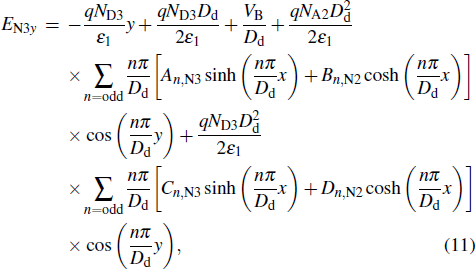
Similarly, the Eijx = ∂Vij/∂x is derived. Obviously, the electric field generated by the coupling components and reversed voltage is easily obtained.

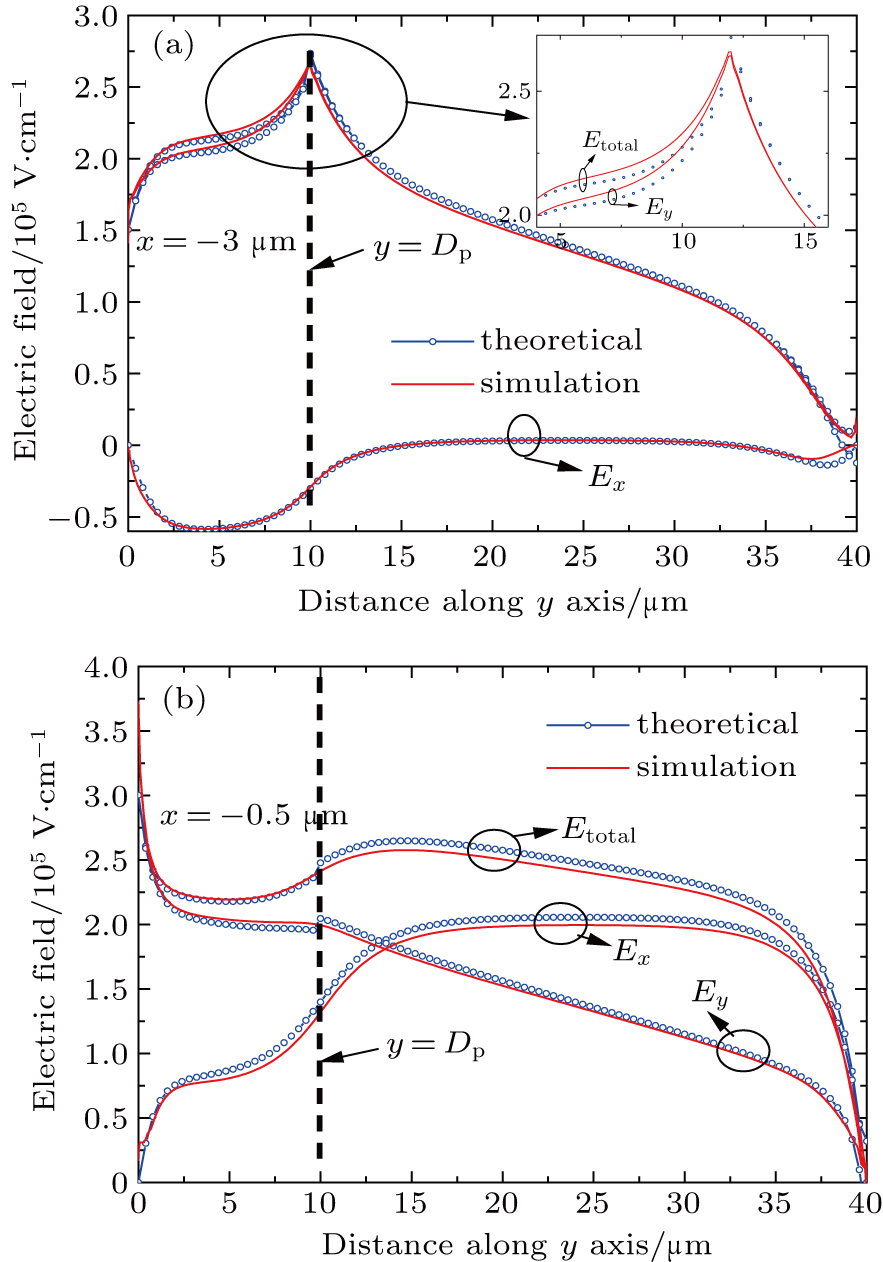
Figure 5 shows the distributions of the electric field based on the analytical model and the Medici simulation results for the HKP-VDMOS. As shown in the figure, the x- and the y-components of the electric field (Ex and Ey) and the total electric field (Etotal) are also indicated.

Fig. 5. (color online) (a) Electric field distributions along the y axis at location x = −3 μm based on the analytical model and Medici simulation results. (b) Electric field profile along the y axis at location at x = −0.5 μm. Length of drift region (Dd) is 40 μm, P1-region doping concentration is 4 × 1015 cm−3, N1-region doping concentration is 5 × 1014 cm−3, N2-region doping concentration is 9 × 1015 cm−3, and relative permittivity of the HK insulator is 200.

The values of ΔEyEy = Ey, HKP − Ey, CHK) and ΔBVyBVy = BVy, HKPBVy, CHK) ΔBVy at the locations x = −0.5 μm and x = −3 μm are shown in Fig. 6. In HKP-VDMOS, Ey is much larger than that in CHK-VDMOS except y < 5 μm. The value of BV of the HKP-VDMOS device is enhanced by ΔBVy = 76 V. The electric field given by the MEDICI simulation results is in very good agreement with that presented by the analytical model results.

Fig. 6. (color online) Variations of ΔEy and ΔBVy at locations x = −0.5 μm and x = −3 μm with distance along the y aixs. Length of drift region (Dd) is 40 μm, P1-region doping concentration is 4 × 1015 cm−3, N1-region doping concentration is 5 × 1014 cm−3, and relative permittivity of the HK-region is 200.
3.4. BV and Ron,sp

Based on the aforementioned Poisson solution, the breakdown voltage can be calculated along the avalanche breakthrough path. The avalanche breakdown condition is given as , where α = 1.8 × 10⁻³⁵E7 cm−1 is the ionization rate and E is the electric field distribution along the breakthrough path. By integrating the impact ionization rate with Fulop’s law, the optimized breakdown voltage is obtained as Eq. (14).

The y-component of the electric field in the device is generally affected by the P-region. The optimized breakdown voltage (BV/V) could be approximated by

Table 2.

Correlation coefficients.

.

Using the relationship between the resistivity and the doping concentration, the ideal on-resistance equation could be rewritten as follows:[16]

where an effective doping concentration Neff is given by
A model to estimate specific on-resistance (Ron,sp/mΩ · cm2) could be approximated by

Table 3.

Correlation coefficients.

.

BV and Ron,sp are closely related to the doping concentrations of the drift region and P-region. In addition, BV is strongly related to the permittivity of the HK insulator. Therefore, the optimized breakdown voltage and specific on-resistance could be predicted by Eqs. (14) and (17), respectively.

The theoretical and simulated results of BV and Ron,sp are each as a function of ND2 in HKP-VDMOS and CHK-VDMOS are shown in Fig. 7(a). As ND2 increases, BV of the HKP-VDMOS can decrease much more than that of CHK-VDMOS. The Ron,sp of HKP-VDMOS fleetly decreases with the increase of ND2, although the Ron,sp of the HKP-VDMOS is slightly higher than that of CHK-VDMOS when ND2 < 9 × 1015 cm−3. The analytical results are in agreement reasonably well with simulations (within 10% of error). Figure 7(b) shows the BV and Ron,sp for HKP-VDMOS at different concentrations of the P1-region (NA). The BV of the HKP-VDMOS increases more than 500 V, and then decreases with increase of NA at each of the ND2 values: 8 × 1015 cm−3, 9 × 1015 cm−3, and 1 × 1016 cm−3. The theoretical errors of BV and Ron,sp are less than 3.2% and 1.3%, respectively, when ND2 = 9 × 1015 cm−3. The optimized BV and Ron,sp versus κ value for the HKP-VDMOS and CKP-VDMOS are demonstrated in Fig. 7(c). With the increase of the κ value, optimized BV increases and optimized Ron,sp decreases both in HKP-VDMOS and CHK-VDMOS. However, the HKP-VDMOS has a superior BV-Ron,sp trade-off relationship. Meanwhile, the theoretical results are in good agreement with simulated results within an error range between 0.5% and 3%.

Fig. 7. (color online) Characteristics of BV and Ron,sp for the CHK-VDMOS and the HKP-VDMOS based on the theoretical result. (a) BV and Ron,sp versus N2-drift doping concentration (ND2), length of drift region (Dd) is 40 μm, N1-region doping concentration is 5 × 1014 cm−3, and relative permittivity of HK-region is 200; (b) BV and Ron,sp versus P1-region doping concentration (NA), and N1-region doping concentration is 5 × 1014 cm−3; (c) BV and Ron,sp versus relative permittivity κ and N1-region doping concentration is 5 × 1014 cm−3.
4. Discussion on optimization results
4.1. Static characteristics

Figure 8(a) shows that the FOMs of the CHKVDMOS and HKP-VDMOS first increase up to a maximum FOM value, and then decrease with the increase of ND2. The maximum FOM of HKP-VDMOS is 31.2 MW/cm2 with Ron,sp of 11.5 mΩ · cm2 at ND2 = 9 × 1015 cm−3 and ND1 = 5 × 1014 cm−3, meanwhile the maximum one of CHK-VDMOS is 25.7 MW/cm2. Figure 8(a) also indicates that when the values of ND2 are 8 × 1015 cm−3, 9 × 1015 cm−3, and 1 × 1016 cm−3, the max FOMs of HKP-VDMOS can also be obtained. With the increase of the κ value, FOMs both increase in HKP-VDMOS and CHK-VDMOS, as given in Fig. 8(c). The FOM of the HKP-VDMOS is much higher than that of the CHK-VDMOS.

Fig. 8. (color online) FOM characteristics of the CHK-VDMOS and the HKP-VDMOS. (a) FOMs versus P1-region doping concentration (NAa) of the HKP-VDMOS and the CHK-VDMOS. FOMs versus N2-drift doping concentration (ND2) of the HKP-VDMOS and the CHK-VDMOS. Length of the drift region (Dd) is 40 μm, N1-region doping concentration is 5 × 1014 cm−3. The relative permittivity of the HK-region is 200. (b) FOMs versus relative permittivity of insulator κ of the HKP-VDMOS and the CHK-VDMOS, and N1-region doping concentration is 5 × 1014 cm−3.

Figure 9 gives plots of Ron,sp versus BV of the HKP-VDMOS and CHK-VDMOS at κ = 100 and κ = 200, respectively. It is noted that the HKP-VDMOS has much lower values of Ron,sp at both κ = 100 and κ = 200 than CHK-VDMOS. Moreover, the well-known law Ron,sp = 5.93 × 10⁻⁹(BV)2.5 of the ideal silicon limit[17] serves as a break-through limit by HKP-VDMOS and CHK-VDMOS. Figure 9 also shows that the HKP-VDMOS has a better performance than other higk-κ MOSFET devices which have been published.

Fig. 9. (color online) Plots of on-resistance Ron,sp versus BV of the HKP-VDMOS and the CHK-VDMOS for relative permittivity of the insulator κ = 100 and 200. The ideal silicon limit on the Ron,sp versus BV is also shown.
4.2. Transient characteristics

Figure 10(a) shows that gate charge (Qgd = 79 nC) in the HKP-VDMOS compared with Qgd = 113 nC in the CHK-VDMOS. The gate charge in the HKP-VDMOS is about 30% reduction in comparison with that in the CHK-VDMOS. The reduction of gate charge can be understood as follows. In the CHK-VDMOS, the gate, drain and N1-region form capacitance C1, and the gate, drain and N2-region form capacitance C2. Furthermore, capacitances C1 and C2 are connected in parallel. However, in HKP-VDMOS, part of the C1 is changed into gate-source capacitance, and thus HKP-VDMOS has much smaller gate–drain capacitance than CHK-VDMOS. Therefore, the Qg of the HKP-VDMOS is smaller than that of the CHK-VDMOS. Figure 10(b) shows the turn-off processes of HKP-VDMOS and CHK-VDMOS. A bias of 500 V connected in series with 50 Ω is applied to each of the drains of HKP-VDMOS and CHK-VDMOS with a gate turning off from 15 V to 0 V. These results show that the values of turn-off time (toff) of HKP-VDMOS and CHK-VDMOS are 68 ns and 79 ns, respectively. It is about 14% enhancement in the HKP-VDMOS compared with that in the CHK-VDMOS. The optimized values of the HKP-VDMOS and the CHK-VDMOS are shown in Tables 4 and 5.

Fig. 10. (color online) Comparisons between the HKP-VDMOS and the CHK-VDMOS. (a) Gate-charging-transient curves for 10-mA gate-charging current. (b) Drain voltage and drain current during the turn-off transient. Length of the drift region (Dd) is 40 μm, P1-region doping concentration is 4 × 1015 cm−3, and relative permittivity of HK-region is 200.
Table 4.

Optimized values of the HKP-VDMOS device and the CHK-VDMOS device.

.
Table 5.

Optimized values of the HKP-VDMOS device and the CHK-VDMOS device.

.
5. Conclusions

An improved vertical power MOSFET with p-region and HK insulator has been proposed and investigated. A P-region is introduced into the drift region for enhancing BV and reducing Ron,sp. Hence, a much higher FOM of HKP-VDMOS than that of CHK-CDMOS can be obtained. The simulation results show that the improved device enables a 16.7% reduction in Ron,sp, and 18% improvement in FOM under the same breakdown voltage (BV), compared with the CHK-VDMOS. An analytical model of the HKP-VDMOS is also derived, and presents the results in good agreement with simulated results.

Reference
[1] Chen X B Huang M M 2012 IEEE Trans. Electron Dev. 59 2430
[2] Lyu X J Chen X B 2013 IEEE Trans. Electron Dev. 60 1709
[3] Yi B Lin Z Chen X 2014 Superlattices & Microstructures 75 278
[4] Zhai D Y Zhu J Zhao Y Cai Y F Shi Y Zheng Y L 2015 Chin. Phys. 24 077201
[5] Zhai D Y Zhao Y Cai Y F Shi Y Zheng Y D 2014 Acta Phys. Sin. 63 127201
[6] Wang P Luo X R Jiang Y H Wang Q Zhou K Wu L J Wang X W Cai J Y Luo Y C Fan Y Hu X R Fang Y H Wei J Zhang B 2013 Chin. Phys. 22 027305
[7] Fan J Wang Z G Zhang B Luo X Y 2013 Chin. Phys. 22 048501
[8] Luo X R Cai J Y Fan Y Fan Y H Wang X W Wei J Jang Y H Zhou K Yin C Zhang B Li Z J Hu G Y 2013 IEEE Trans. Electron Dev. 60 2840
[9] Mao W Wang H Y Wang X F Du M Zhang J F Zheng X F Wang C Ma X H Zhang J C Hao Y 2017 Chin. Phys. 26 047306
[10] Li W Zheng Z Wang Z G Li P Fu X J He Z R Liu F Yang F Xiang F Liu L C 2017 Chin. Phys. 26 017701
[11] Naugarhiya A Kondekar P N 2015 Superlattices & Microstructures 83 310
[12] Huang M Chen X 2015 Superlattices & Microstructures 88 244
[13] Napoli E Wang H Udrea F 2008 IEEE Electron Dev. Lett. 29 249
[14] Wang H Napoli E Udrea F 2009 IEEE Trans. Electron Devices 56 3175
[15] Tamaki T Nakazawa Y Kanai H Abiko Y Ikegami Y Ishikawa M Wakimoto E Yasuda T Eguchi S 2011 IEEE International Symposium on Power Semiconductor Devices and ICS 308
[16] Baliga B J 2008 Fundamentals of power semiconductor devices Beijing Science Press 100 104 10.1007/978-0-387-47314-7
[17] Duan B Yang Y 2011 IET Micro & Nano Lett. 6 777
[18] Naugarhiya A Kondekar P N 2013 IEEE International Conference on Control, Automation, Robotics and Embedded Systems 1
[19] Zhou J Huang C F Cheng C H Zhao F 2016 IEEE Trans. Electron Dev. 63 2255
[20] Takahashi K Kuribayashi H Kawashima T Wakimoto S Mochizuki K Nakazawa H 2006 IEEE International Symposium on Power Semiconductor Devices and Ic’s 1
[21] Wu L J Zhang Z J Song Y Yang H Hu L M Yuan N 2017 Chin. Phys. 26 027101