

Mechanism of single-event transient pulse quenching between dummy gate isolated logic nodes*
Cite this Article
Chen Jian-Jun, Chi Ya-Qing, Liang Bin. Mechanism of single-event transient pulse quenching between dummy gate isolated logic nodes* . Chinese Physics B, 2014, 24(1): 016102 
Permissions
Mechanism of single-event transient pulse quenching between dummy gate isolated logic nodes*
Corresponding author. E-mail: cjj192000@163.com
Project supported by the National Natural Science Foundation of China (Grant No. 61376109) and the Opening Project of National Key Laboratory of Science and Technology on Reliability Physics and Application Technology of Electrical Component, China (Grant No. ZHD201202).
Abstract
As integrated circuits scale down in size, a single high-energy ion strike often affects multiple adjacent logic nodes. The so-called single-event transient (SET) pulse quenching induced by single-event charge sharing collection has been widely studied. In this paper, SET pulse quenching enhancement is found in dummy gate isolated adjacent logic nodes compared with that isolated by the common shallow trench isolation (STI). The physical mechanism is studied in depth and this isolation technique is explored for SET mitigation in combinational standard cells. Three-dimensional (3D) technology computer-aided design simulation (TCAD) results show that this technique can achieve efficient SET mitigation.
Keyword:
61.80.Jh; 85.30.Tv; 85.30.Pq; single-event transients (SETs); dummy gate isolation; SET pulse quenching; radiation hardened by design (RHBD)
1. Introduction
As circuit dimensions keep scaling down, the use of integrated circuits (ICs) in space environment presents a lot of challenges which arise from their increasing susceptibility to soft errors.[1– 3] The major sources of the soft errors are single-event transients (SETs) and single-event upsets (SEUs), which may be induced when an ion strikes the sensitive region of an IC.
The extreme reduction in minimum transistor-to-transistor spacing has resulted in multiple transistors being affected by a single ion strike, and the charge sharing collection between adjacent logic nodes has become a universal phenomenon. Depending on the exact relationship between adjacent logic nodes, the charge sharing collection can play a beneficial role in SET mitigation.[4– 6] The logic nodes of ICs in close proximity are usually electrically related, when these electrically coupled nodes collect charge simultaneously, SET pulse quenching can reduce the overall SET pulse width (WSET) or completely eliminate SET, [6] resulting in reducing vulnerability to SETs in the ICs. The previous work has demonstrated that the circuit layout topology has a significant influence on SET, consequently, several novel layout techniques have been explored for SET mitigation via layout improvement.[6– 10] However, in those investigations, the area of cells that use such improved layouts is significantly increased, and the electrical characteristics of the cell are also changed. The dummy gate has also been explored for SEU mitigation[11] and analog SET mitigation, [12] but the potential of this dummy gate on digital SET mitigation still needs to be studied.
In this paper, the SET pulse quenching enhancement is found in a new layout technique. In the layout, a shallow trench isolation (STI) is replaced by a dummy gate in order to isolate the adjacent nodes. We first discover the reason why SET pulse quenching is enhanced in this new technique for the case of adjacent inverters, and then explore its effect on SET mitigation in some special combinational logic cells that are composed of two stages.
2. Dummy gate isolation technique
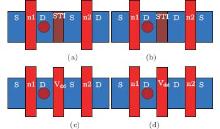
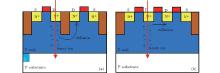
As shown in Figs. 1(a) and 1(b), for adjacent inverters, two adjacent P-channel metal oxide semiconductor field effect transistors (PMOSs) or N-channel metal oxide semiconductor field effect transistors (NMOSs) have two regular layout placements (referred to as layout 1 and layout 2: the source (S) and the drain (D) have different placements). In these traditional layout placements, two adjacent sensitive regions are generally isolated by an STI. In the present paper, we introduce a new technique to isolate the two sensitive regions which involves a dummy gate (the power supply voltage Vdd is connected to the gate for PMOS and the ground supply voltage Vss is connected to the gate for NMOS). The approach is illustrated in Figs. 1(c) and 1(d) and will be referred to as layout 3 and layout 4. In the proposed layout, the addition of the dummy gate has no net effect on the circuit function and appears to have a negligible influence in light of the circuit-level single-event hardened design.
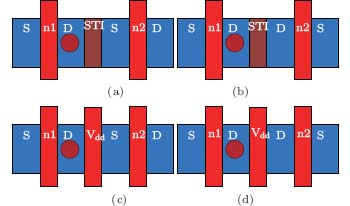 | Fig. 1. Four different layout placements for adjacent PMOS circuits in adjacent inverters: (a) layout 1, (b) layout 2, (c) layout 3, (d) layout 4. |
Three-dimensional (3D) mixed-mode technology computer aided design simulation (TCAD) has been proven to be a useful method for investigating the mechanism of single-event effects, the validation of the simulation methodology has been widely proven in the previous studies, and many important conclusions or predictions[13– 16] were also based solely on the TCAD simulations. In our present work, Sentaurus TCAD vE-2010.12 from Synopsys is adopted to perform the simulation. The 90 nm twin-well bulk CMOS technology is used, and the doping profiles of the devices are calibrated according to a commercial process. The gate width W and length L refer to the sizes of the inverter standard cell, the W/L ratio of NMOS is 400 nm/100 nm, and that of PMOS is 600 nm/100 nm. The N well contact distance from PMOS is 0.38 μ m, and the P well contact distance from NMOS is also 0.38 μ m.
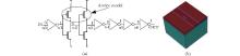
The simulation is performed in a seven-inverter chain (shown in Fig. 2(a)). For the P-hit case, two adjacent PMOSs in the second and the third inverters are modeled by a TCAD numerical model (shown in Fig. 2(b)), the other transistors are modeled as integrated circuit emphasis (SPICE) circuit models in the simulation program. For the N-hit case, the method is similar. Ions strike at the center of the drain of the second PMOS (or NMOS) and proceed through the device on a 10 μ m× 10 μ m × 10 μ m substrate. Like the setup described in Ref. [6], a backside substrate contact is used along the bottom surface of the substrate, connected in series with a 1 kΩ resistor. After ions strike through the device, SETs are produced and propagate though the inverter chain. The pulse widths at the terminal of the chain are then calculated.
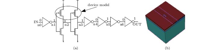 | Fig. 2. Circuit used for SET production and propagation: (a) circuit, (b) device model. |
As in the previous studies, [6– 10] heavy ion strikes are simulated via an electron– hole pair column, with the ion track taken as its axis. The linear energy transfer (LET) value is kept constant along the heavy ion track. The length and the radius of the ion track are 10 μ m and 0.1 μ m, respectively.
The following physical models are used: (i) Fermi– Dirac statistics, (ii) the effect of band-gap narrowing, (iii) doping dependent Shockley– Read– Hall (SRH) recombination and Auger recombination, (iv) the effects of doping, electric field, carrier– carrier scattering, and interface scattering on mobility, and (v) a hydrodynamic model used for carrier transport. Unless otherwise specified, the default models and parameters provided by Sentaurus TCAD are used.
3. Simulation results and discussion
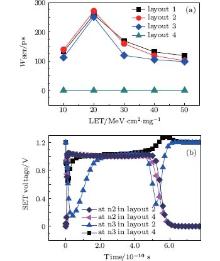
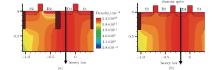
For the hit PMOS (P-hit) case, our simulation results are presented in Fig. 3. In Fig. 3(a), it can be seen that the SETs disappear entirely in layout 4 for all simulations, and that the typical WSET in layout 3 is also smaller than that found in the traditional layouts (layout 1 and layout 2). The SET pulse waveforms at nodes n2 and n3 are shown in Fig. 3(b) for layout 2 and layout 4 (LET = 50 MeV· cm2/mg), the data indicate that the pulse quenching appears in all of these layout placements for PMOS circuits.
 | Fig. 3. P-hit SET produced in the four different layouts: (a) SET pulse widths, (b) SET pulse waveforms in layout 2 and layout 4. |
When an initial large SET is present at n2, the state of n2 changes from 0 to 1, and the third dummy NMOS becomes an on-state one, which will discharge the charge at n3 and cause the state of n3 to change from 1 to 0. Due to the charge sharing collection, the third PMOS may also collect ion-induced charge to compensate for the charge at n3, thus preventing the state of n3 from going from 1 to 0. The competition between these two processes leads to a shorter SET (or even to the elimination of the SET) appearing at n3 and finally at the terminal of the chain. This effect was firstly discovered by Ahlbin et al. and is known as the pulse quenching.[5] Owing to this quenching, the initial large SET is partially reduced or completely eliminated, and any enhancement of the charge sharing collection can enhance the pulse quenching and thus may be an efficient means to reduce the single-event vulnerability for ICs.
For the hit NMOS (N-hit) case, the simulation results are shown in Fig. 4, as before, WSET is generally small in the proposed layouts (layout 3 and layout 4) compared with those in the traditional layouts (layout 1 and layout 2). We also find that the smallest SETs of all layouts are present in layout 4. The SET pulse waveforms at nodes n2 and n3 are also shown in Fig. 4(b) for layout 2 and layout 4 (LET = 50 MeV· cm2/mg). The pulse quenching does not occur in the traditional layouts nor in layout 3, so a large SET at n2 directly propagates to the next node n3. While in layout 4, the pulse quenching appears in the circuit and the SET pulse width is significantly reduced at node n3, as shown in Fig. 4(b).
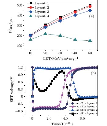 | Fig. 4. N-hit SET produced in the four different layouts: (a) SET pulse widths, (b) SET pulse waveforms in layout 2 and layout 4. |
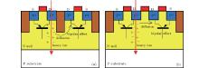
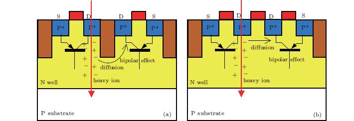
The underlying mechanism in the P-hit charge collection involves the parasitic bipolar effect, which is activated by the disturbance of the N well potential. As shown in Fig. 5, after an ion strikes through the device, numerous electron– hole pairs are produced along the ion track. The reverse-biased P– N junction between the P substrate and the N well is favorable to prevent these ionized electrons from dispersing into the substrate, so a number of surplus electrons are left behind in the N well, which results in a falling N well potential. This causes the P– N junction between the P+ source and the N well to become forward-biased. As a result, a source– channel– drain parasitic P+ NP+ bipolar junction transistor (BJT) is activated, which will cause a number of holes to be injected into the source (which acts as the emitter in the parasitic BJT). Then, these holes are collected at the drain (acting as the collector in the parasitic BJT) after they have passed through the channel (i.e., the base of the parasitic BJT).
 | Fig. 5. Main mechanisms for underlying adjacent PMOS charge sharing collection in (a) layout 2 and (b) layout 4. |
As illustrated in Fig. 5, in layout 2, an ion strike can affect the adjacent N well potential even though the two drains are isolated by an STI, because the bipolar effect is still active, the adjacent drain is also able to collect the source-injected holes. Therefore, the pulse quenching can also appear in the common layout placements. In our proposed layout 4, ion-induced charge can directly diffuse to the adjacent PMOS, leading to an enhanced bipolar effect; on the other hand, the ion-induced holes can also be directly collected by the adjacent drain, which leads to a significantly enhanced charge sharing collection in layout 4, so the pulse quenching is also greatly enhanced (as shown in Fig. 5(b)). In order to further verify that both the diffusion and the bipolar effect are enhanced in the proposed layout 4, the distribution of hole density along the channel cross section at 50 ps after the ion striking is simulated. As shown in Fig. 6, 50 ps after the ion striking, the ion-induced holes can directly diffuse to the adjacent node in layout 4, while the holes cannot diffuse to the adjacent node due to the isolation of the STI in layout 2, so the diffusion is enhanced in layout 4. Moreover, the source injected holes in layout 4 are also more than those in layout 2, so the bipolar effect is also enhanced in layout 4.
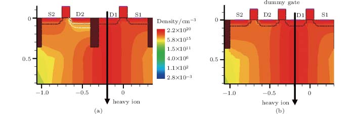 | Fig. 6. Distributions of hole density along the channel cross section at 50 ps after the ion striking in (a) layout 2 and (b) layout 4. |
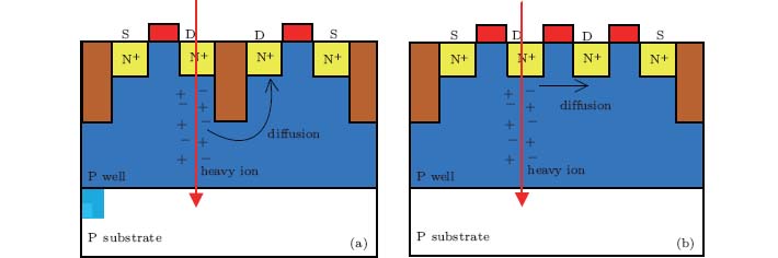
In N-hit charge collection, the main process at work is diffusion. Contrary to what takes place in PMOS devices, here the weak P– N junction between the P well and the P substrate cannot prevent ionized holes from dispersing into the substrate, so the holes can easily diffuse throughout the entire substrate, resulting in an avoidance of forward bias of the P– N junction between the N+ source and the P well. Since the source cannot inject electrons, the electrons collected at the drain come only from the ion-induced electron population.
Figure 7 illustrates what occurs in NMOS devices. In layout 2 (Fig. 7(a)), the two drains are isolated by an STI, when an ion strikes the left drain, the ion-induced electrons must pass through the trench before they can be collected by the right drain. As a result, the number of electrons collected by the right drain is insignificant, implying that the pulse quenching is insignificant in NMOS circuits. However, in our proposed layout 4 (Fig. 7(b)), the two drains are located in the same active area, as a consequence, when an ion strikes through one drain, the ion-induced electrons can diffuse directly towards the other drain and be readily collected. Therefore, the charge sharing collection is enhanced in this design, and the pulse quenching is evident in NMOS circuits of this layout.
 | Fig. 7. Main mechanisms for underlying adjacent NMOS charge sharing collection in (a) layout 2 and (b) layout 4. |
4. RHBD layout technique
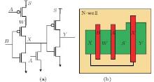
As mentioned in Ref. [6], some special logic cells (such as the OR cell shown in Fig. 8(a)) are composed of two stages, where the output of the first stage is connected to the input of a following inverting stage. In these kinds of logic cells, charge collection sharing between the two adjacent logic nodes can efficiently mitigate SETs, owing to the pulse quenching. Using our dummy gate isolation technique, we propose additional novel layout placements to achieve SET mitigation for these logic cells.
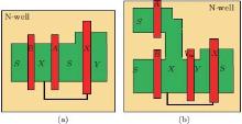
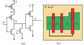 | Fig. 8. (a) Schematic of OR cell, and (b) the layout of the PMOS circuits of an OR2X1 cell (layout 5). |
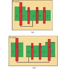
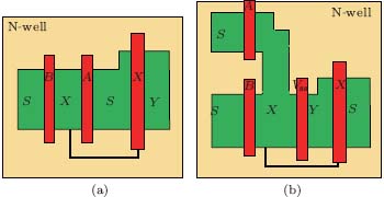
For the P-hit case, the OR cell serves as a simple example for the present study. As shown in Fig. 8(b), in our design, the two drain regions (referred to as X and Y regions in the layout) are intentionally located very close to each other, but these two regions are then isolated from each other by a dummy gate as shown in Fig. 9(a). For the sake of comparison, the layout placement presented in Ref. [6] is also used to carry out simulations, which is shown in Fig. 9(b). These different layouts are referred to as layout 5, layout 6, and layout 7, respectively.
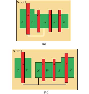 | Fig. 9. The OR2X1 cells of (a) the proposed layout (layout 6) and (b) the layout described in Ref. [6] (layout 7). |
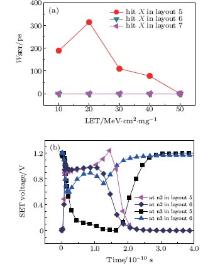
In our simulations, an OR2X1 cell is struck in the X and W regions by an ion at normal incidence, and a six-inverter chain is connected to the output of the cell. LETs of 10 MeV· cm2/mg, 20 MeV· cm2/mg, 30 MeV· cm2/mg, 40 MeV· cm2/mg, and 50 MeV· cm2/mg are simulated. As shown in Fig. 10(a), when ions strike the X region, SETs appear in layout 5 but not in layout 6 nor in layout 7. The SET pulse waveforms at nodes n2 and n3 are shown in Fig. 10(b) for layout 5 and layout 6 (for an LET of 10 MeV· cm2/mg), they indicate that the enhancement of the pulse quenching plays a key role in SET mitigation in the new layouts. When the LET of 50 MeV· cm2/mg is simulated, the pulse also disappears in layout 5, owing to the quenching that is enhanced with increasing LET.
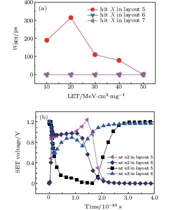 | Fig. 10. Simulated (a) SET pulse widths (hit the X region), and (b) SET pulse waveforms in layout 5 and layout 6 (LET = 10 MeV· cm2/mg, ions strike at the X region). |
When ions strike the W region, the SETs disappear in all three layouts. In layout 5, where the W region is close to the Y region, the pulse quenching is more significant, so no SET appears in the circuits. In layout 6 and layout 7, where the pulse quenching is enhanced as a result of the clever layout design, the SETs do not appear in the circuits either.
For the P-hit case, both layout 6 and layout 7 are efficiently hardened to the effects of SETs. However, the area penalty in layout 6 is smaller than that in layout 7. Moreover, the PMOS drain area of the second stage is increased in layout 7, which not only changes the output rise time and fall time, but also leads to an actual increase in single even (SE) vulnerability for the second stage.[6]
For the N-hit case, the layout of NMOS circuits in an AND cell (shown in Fig. 11) has a similar topology to that of the PMOS circuit in an OR cell. We simulate SETs for different layout placements, similar to what was done for the layouts in Fig. 9. The results are shown in Fig. 11.
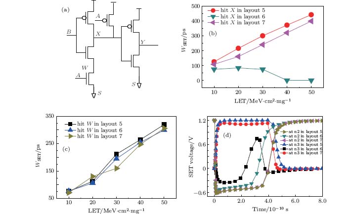 | Fig. 11. (a) Schematics of simulated AND cell, (b) the hitting X region case, (c) the hitting W region case, (d) SET pulse waveforms in layout 5, layout 6, and layout 7 (LET = 50 MeV· cm2/mg, ions strike at the X region). |
In our simulations, an AND2X1 cell is struck in the X and W regions by ions at normal incidence, and a six-inverter chain is connected to the output of the cell. LETs of 10 MeV· cm2/mg, 20 MeV· cm2/mg, 30 MeV· cm2/mg, 40 MeV· cm2/mg, and 50 MeV· cm2/mg are simulated. As shown in Fig. 11, when ions hit the X region, WSET is significantly reduced in layout 6, as a result of the pulse quenching. However, pulse quenching does not occur in layout 5 nor in layout 7 (Fig. 11(b)). When the W region is struck, WSET in layout 6 is also smaller than that in layout 5, which is shown in Fig. 11(c).
The WSET in layout 7 is found to be smaller than that in layout 5 in all our simulations, however this is not due to the pulse quenching. As shown in Fig. 11(d), an SET at n2 in layout 5 is almost identical to the SET in layout 7, but the SET pulse at n3 is reduced in the fall time region for layout 7. The reason for this is that the second stage comprises two NMOSs in layout 7, but only one NMOS in layout 5, so the fall time in layout 7 is quicker than that in layout 5, therefore WSET in layout 7 is smaller than that in layout 5.
For the N-hit case, comparing with the results for layout 5, we can see that layout 6 provides the benefit of greater SET mitigation, as well as has a smaller area penalty.
The layout of NMOS circuits in an OR cell and the layout of PMOS circuits in an AND cell have a similar topology, which allows a similar novel layout to be used for SET mitigation in both scenarios. As with the previously described design, our proposed design is based on a traditional layout (Fig. 12(a)), where the two drain regions are intentionally located close to each other and isolated mutually by a dummy gate (Fig. 12(b)).
 | Fig. 12. Layout placements for PMOS part of an AND cell (or NMOS part of an OR cell, just the N-well is replaced by the P-well): (a) traditional layout, (b) the proposed layout. |
In addition to the case of two-stage logic cells, our layout technique can be extended to two adjacent electrically-related one-stage cells as follows: firstly, the most sensitive adjacent electrically-related nodes in the ICs are evaluated, then the proposed layout may be used to reduce the single-event vulnerability for these most sensitive adjacent logic node pairs.
The performance penalty can be ignored in the new improved layout, because the logic size of the transistor of the cell is not changed. The area penalty is also smaller in the proposed layout than that in other hardening layout techniques, which has been discussed in the previous section. However, in our proposed layout, neither Vdd nor Vss can be directly connected to the gate due to the forbiddance of the electrical rules in the layout design (requiring a guard bridge), so the actual implementation of the proposed layout requires a careful performance of an electrical rule check (ERC).
5. Conclusion
The physical mechanism of SET pulse quenching enhancement is studied in depth in dummy gate isolated adjacent logic nodes. The 3D TCAD numerical simulations show that due to the enhanced pulse quenching, the overall SET pulse width can be partially reduced or completely eliminated, while at the same time producing negligible area and performance penalties. The proposed layout technique can be extended to two-stage logic cells and to two adjacent electrical-related one-stage cells, and it may be used to reduce the single-event vulnerability of ICs.
Reference
| 1 |
|
| 2 |
|
| 3 |
|
| 4 |
|
| 5 |
|
| 6 |
|
| 7 |
|
| 8 |
|
| 9 |
|
| 10 |
|
| 11 |
|
| 12 |
|
| 13 |
|
| 14 |
|
| 15 |
|
| 16 |
|