Mechanism of single-event transient pulse quenching between dummy gate isolated logic nodes

Mechanism of single-event transient pulse quenching between dummy gate isolated logic nodes |
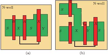
| Fig.#cod#x00A0;12. Layout placements for PMOS part of an AND cell or NMOS part of an OR cell, just the N-well is replaced by the P-well: a traditional layout, b the proposed layout. |
 |