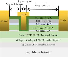
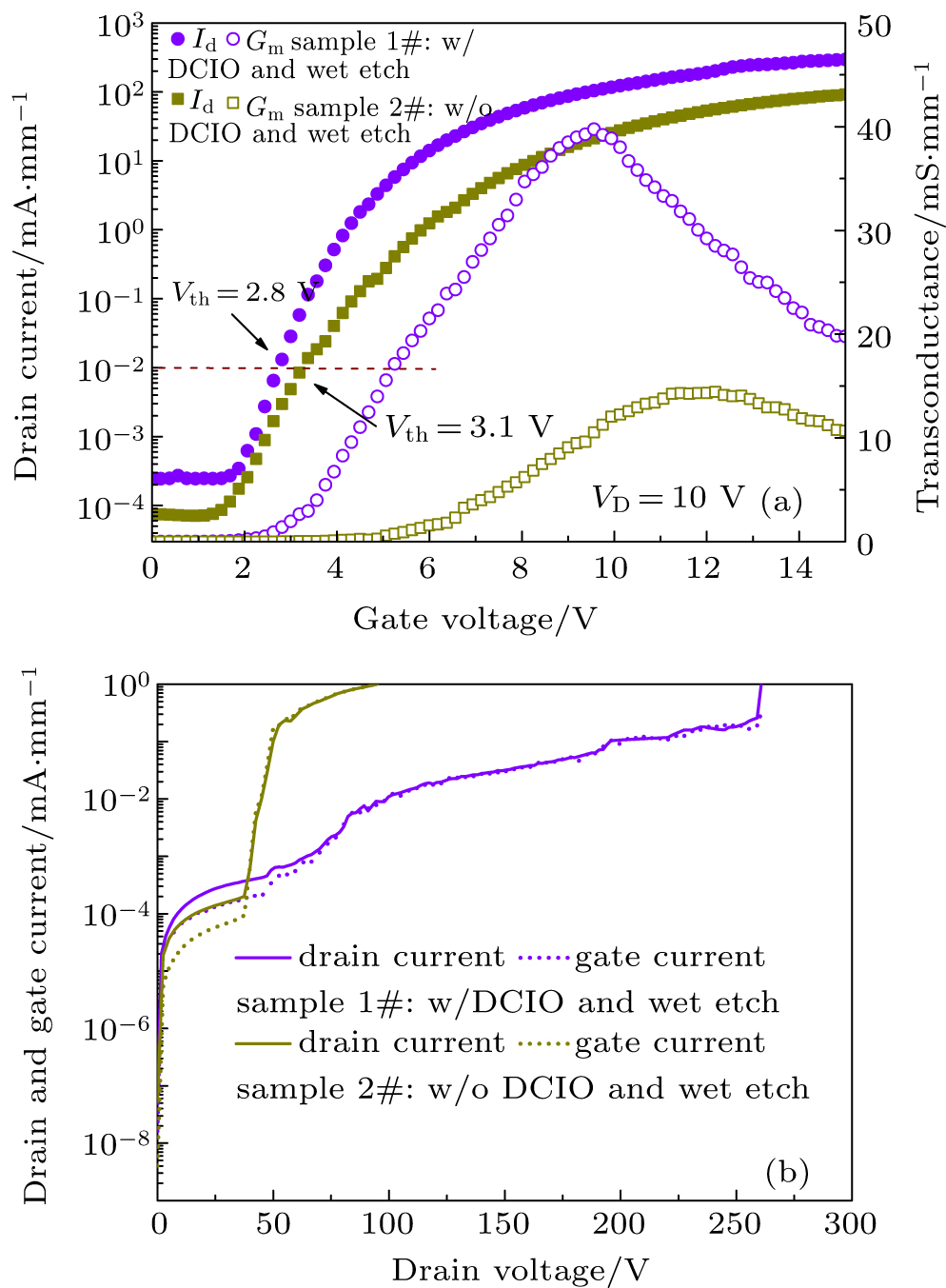
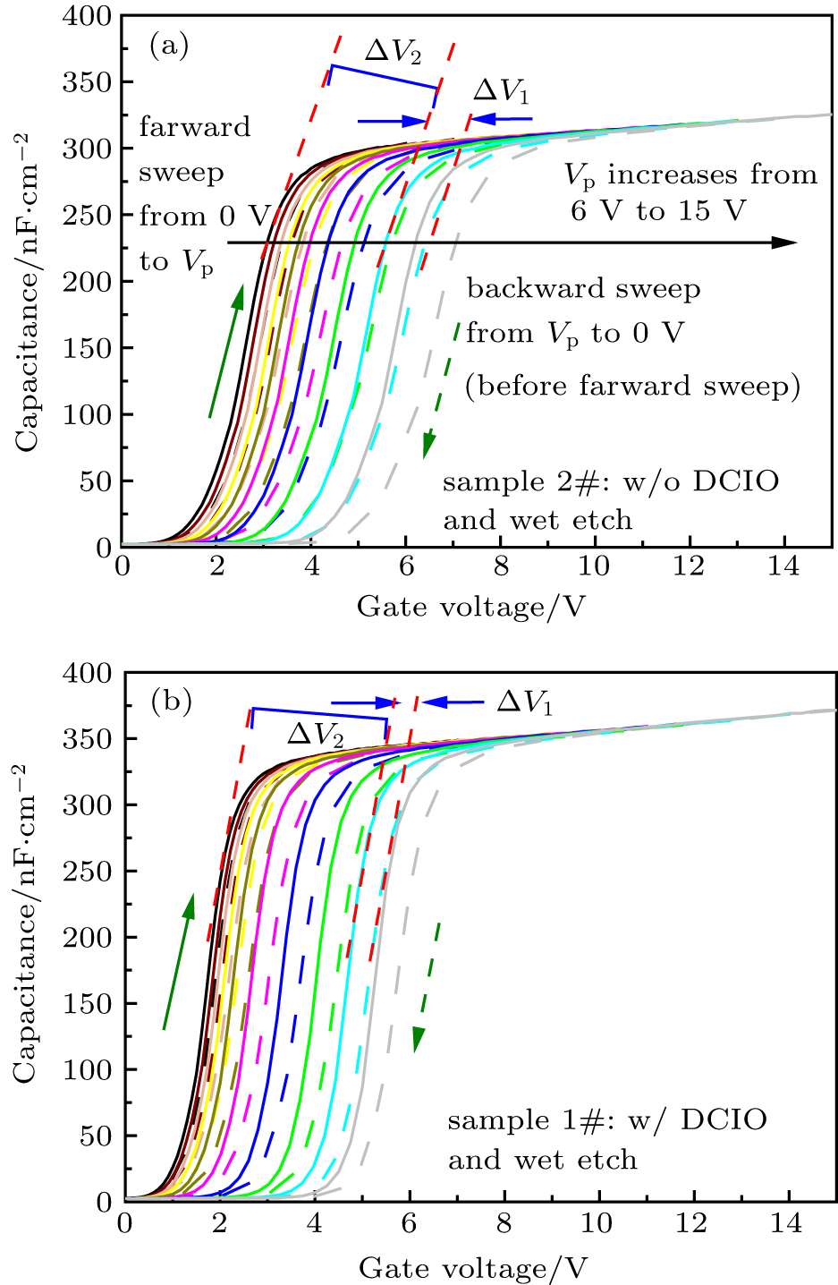
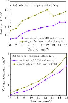
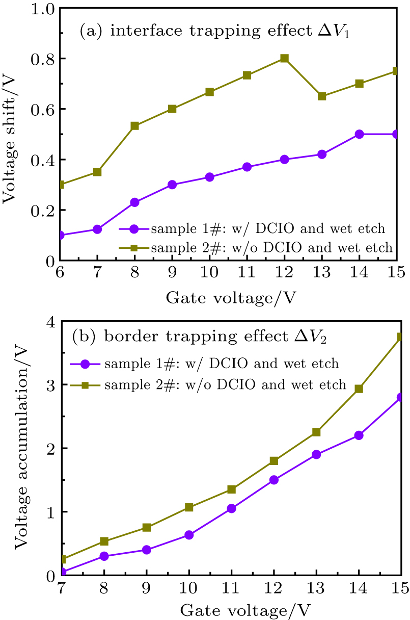
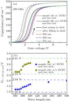
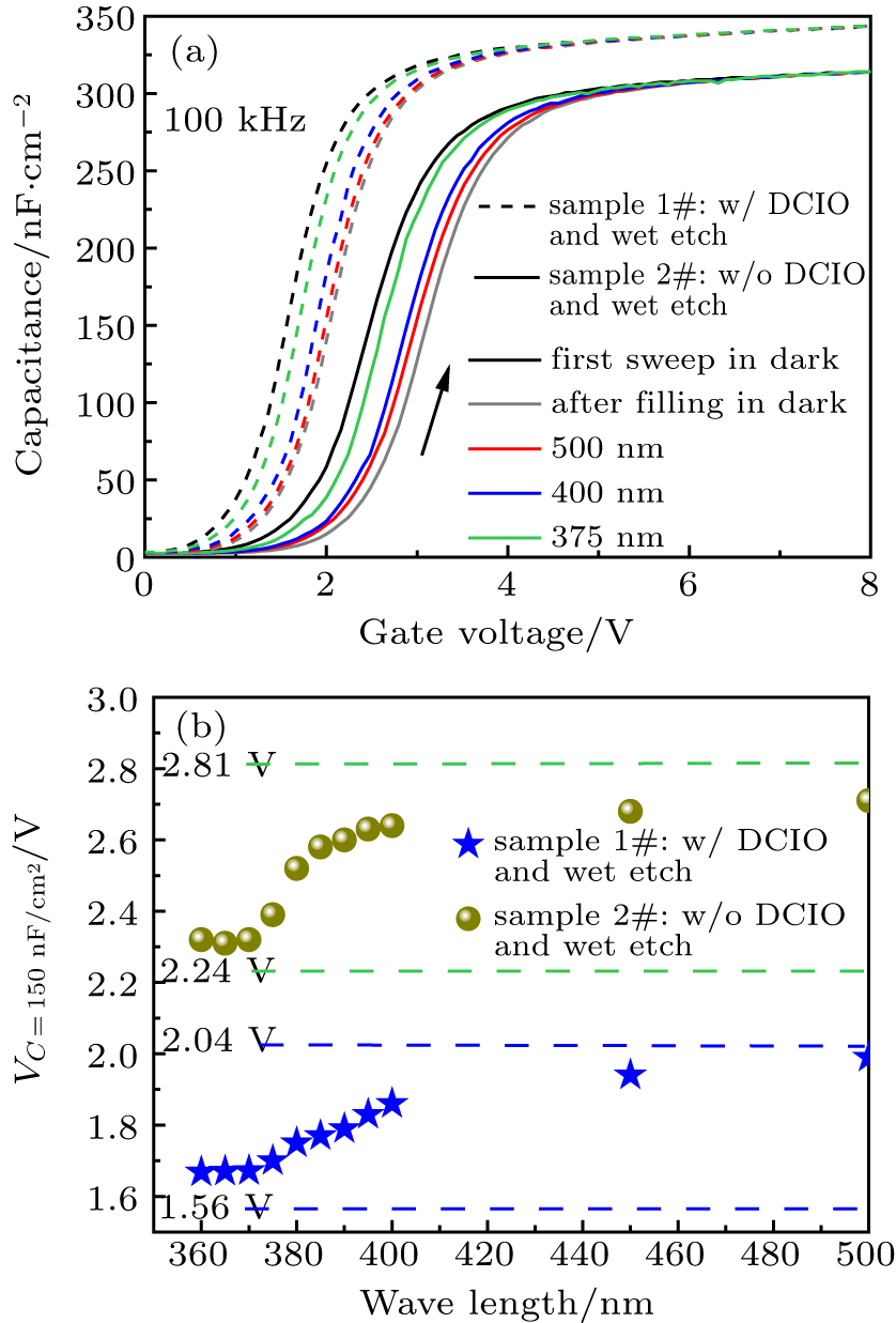
| [1] |
|
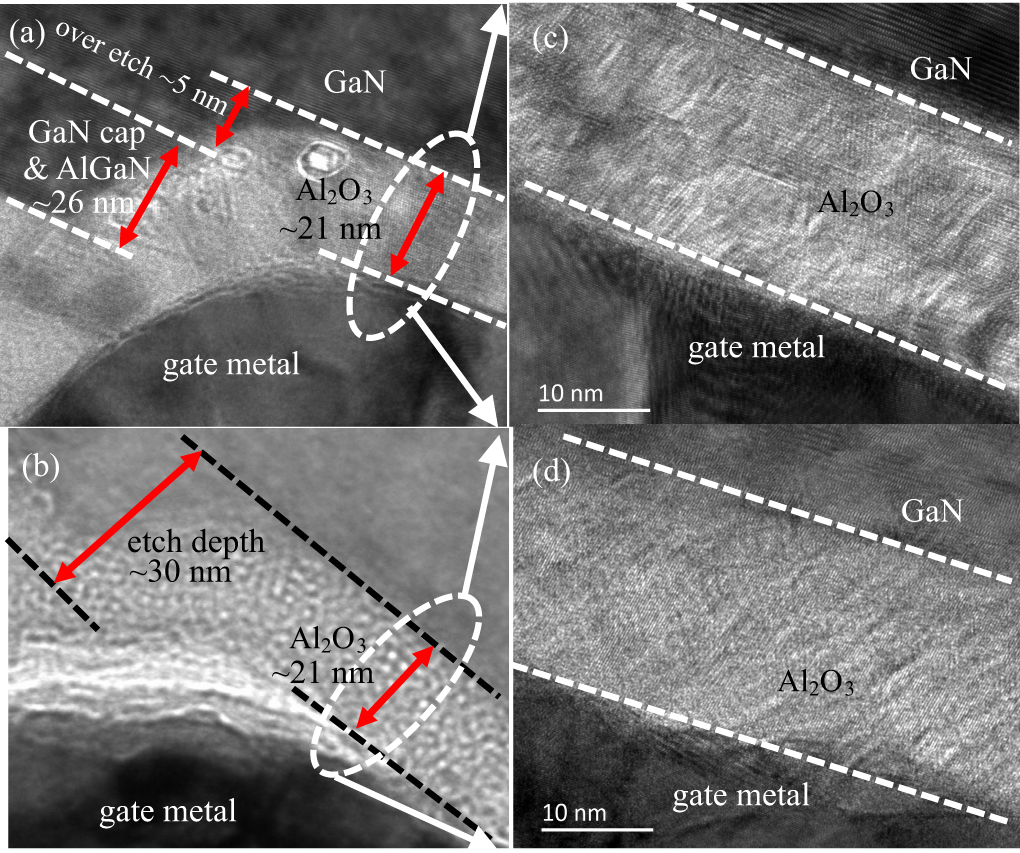
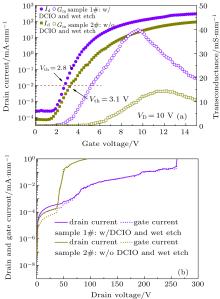
| [2] |
Hou B, Ma X H, Yang L, Zhu J J, Zhu Q, Chen L X, Mi M H, Zhang H S, Zhang M, Zhang P, Zhou X W, Hao Y 2017 Appl. Phys. Express 10 076501 DOI: 10.7567/APEX.10.076501 |
| [3] |
Zheng X F, Wang A C, Hou X H, Wang Y Z, Wen H Y, Wang C, Lu Y, Mao W, Ma X H, Hao Y 2017 Chin. Phys. Lett. 34 27301 DOI: 10.1088/0256-307X/34/2/027301 |
| [4] |
|
| [5] |
Roberts J W, Chalker P R, Lee K B, Houston P A, Cho S J, Thayne I G, Guiney I, Wallis D, Humphreys C J 2016 Appl. Phys. Lett. 108 072901 DOI: 10.1063/1.4942093 |
| [6] |
Hou B, Ma X H, Zhu J J, Yang L, Chen W W, Mi M H, Zhu Q, Chen L X, Zhang R, Zhang M, Zhou X W, Hao Y 2018 IEEE Electron Dev. Lett. 39 397 DOI: 10.1109/LED.2018.2791441 |
| [7] |
Mochizuki K, Mishima T, Terano A, Kaneda N, Ishigaki T, Tsuchiya T 2011 IEEE Trans. Electron. Dev. 58 1979 DOI: 10.1109/TED.2011.2145380 |
| [8] |
Liu Z H, Ng G I, Arulkumaran S, Maung Y K T, Teo K L, Foo S C, Sahmugan-athan V 2009 Appl. Phys. Lett. 95 223501 DOI: 10.1063/1.3268474 |
| [9] |
Ma X H, Zhu J J, Liao X Y, Yue T, Chen W W, Hao Y 2013 Appl. Phys. Lett. 103 033510 DOI: 10.1063/1.4813912 |
| [10] |
Zhou Q, Liu L, Zhang A B, Chen B W, Jin Y, Shi Y Y, Wang Z H, Chen W J, Zhang B 2016 IEEE Electron Dev. Lett. 37 165 DOI: 10.1109/LED.2015.2511026 |
| [11] |
Sang F, Wang M J, Tao M, Liu S F, Yu M, Xie B, Wen C P, Wang J Y, Wu W G, Hao Y L, Shen B 2016 Appl. Phys. Express 9 091001 DOI: 10.7567/APEX.9.091001 |
| [12] |
Zhu J J, Zhu Q, Chen L X, Hou B, Yang L, Zhou X W, Ma X H, Hao Y 2017 IEEE Trans. Electron. Dev. 64 840 DOI: 10.1109/TED.2017.2657780 |
| [13] |
Wang M J, Wang Y, Zhang C, Xie B, Wen C P, Wang J Y, Hao Y L, Wu W G, Chen K J, Shen B 2014 IEEE Trans. Electron. Dev. 61 2035 DOI: 10.1109/TED.2014.2315994 |
| [14] |
Fleetwood D M, Winokur P S, Reber J R A, Meisenheimer T L, Schwank J R, Shaneyfelt M R, Riewe L C 1993 J. Appl. Phys. 73 5058 DOI: 10.1063/1.353777 |
| [15] |
|
| [16] |
Zhu J J, Ma X H, Hou B, Ma M, Zhu Q, Chen L X, Yang L, Zhang P, Zhou X W, Hao Y 2018 IEEE Trans. Electron. Dev. 65 5343 DOI: 10.1109/TED.2018.2874314 |
| [17] |
Yang S, Tang Z K, Wong K Y, Lin Y S, Liu C, Lu Y Y, Huang S, Chen K J 2013 IEEE Electron Dev. Lett. 34 1497 DOI: 10.1109/LED.2013.2286090 |
| [18] |
Partida-Manzanera T, Zaid Z H, Roberts J W, Dolmanan S B, Lee K B, Houston P A, Chalker P R, Tripathy S, Potter R J 2019 J. Appl. Phys. 126 034102 DOI: 10.1063/1.5049220 |
| [19] |
Zhu J J, Ma M, Zhu Q, Hou B, Chen L X, Yang L, Zhou X W, Ma X H, Hao Y 2018 2018 IEEE Workshop on Wide Bandgap Power Devices and Applications in Asia WiPDA Asia May 17–19, 2018 Xi’an, China 135 DOI: 10.1109/WiPDAAsia.2018.8734573 |
| [20] |
Zhu J J, Zhang Y C, Ma X H, Liu S Y, Jing S Q, Zhu Q, Mi M H, Hou B, Yang L, Uren M J, Kuball M, Hao Y 2020 Semiconductor Science and Technology 35 065017 DOI: 10.1088/1361-6641/ab8356 |
| [21] |
Sun H, Wang M J, Yin R Y, Chen J G, Xue S, Luo J S, Hao Y L, Chen D M 2019 IEEE Trans. Electron. Dev. 66 3290 DOI: 10.1109/TED.16 |
| [22] |
|
| [23] |
Zheng X F, Dong S S, Ji P, Wang C, He Y L, Lv L, Ma X H, Hao Y 2018 Appl. Phys. Lett. 112 233504 DOI: 10.1063/1.5024645 |
| [24] |
Liu S H, Yang S, Tang Z K, Jiang Q M, Liu C, Wang M J, Shen B, Chen K J 2015 Appl. Phys. Lett. 106 051605 DOI: 10.1063/1.4907861 |
| [25] |
Qin X Y, Lucero A, Azcatl A, Kim J, Wallace R M 2014 Appl. Phys. Lett. 105 011602 DOI: 10.1063/1.4887056 |
| [26] |
Zhou X Y, Lv Y J, Tan X, Wang Y G, Song X B, He Z Z, Zhang Z R, Liu Q B, Han T T, Fang Y L, Feng Z H 2018 Acta Phys. Sin. 67 178501 in Chinese DOI: 10.7498/aps.67.20180474 |
| [27] |
|
| [28] |
Shen Z, He L, Zhou G L, Yao Y, Yang F, Ni Y Q, Zheng Y, Zhou D Q, Ao J P, Zhang B J, Liu Y 2016 Phys. Status Solidi 213 2693 DOI: 10.1002/pssa.201532785 |
| [29] |
Yatabe Z, Hori Y, Ma W C, Asubar J T, Akazawa M, Sato T, Hashizume T 2014 J. Appl. Phys. 53 100213 DOI: 10.7567/JJAP.53.100213 |
 ), Xin-Chuang Zhang(张新创)1,2, Si-Yu Liu(刘思雨)1,2, Qing Zhu(朱青)1,2, Yue Hao(郝跃)2