Passivation of carbon dimer defects in amorphous SiO2/4H–SiC (0001) interface: A first-principles study
Zhang Yi-Jie1, Yin Zhi-Peng1, Su Yan2, Wang De-Jun1, †
Liaoning Integrated Circuit Technology Key Laboratory, School of Control Science and Engineering, Faculty of Electronic Information and Electrical Engineering, Dalian University of Technology, Dalian 116024, China
School of Physics, Dalian University of Technology, Dalian 116024, China


† Corresponding author. E-mail: dwang121@dlut.edu.cn

Abstract

An amorphous SiO2/4H–SiC (0001) interface model with carbon dimer defects is established based on density functional theory of the first-principle plane wave pseudopotential method. The structures of carbon dimer defects after passivation by H2 and NO molecules are established, and the interface states before and after passivation are calculated by the Heyd–Scuseria–Ernzerhof (HSE06) hybrid functional scheme. Calculation results indicate that H2 can be adsorbed on the O2–C=C–O2 defect and the carbon–carbon double bond is converted into a single bond. However, H2 cannot be adsorbed on the O2 –O2 defect. The NO molecules can be bonded by N and C atoms to transform the carbon–carbon double bonds, thereby passivating the two defects. This study shows that the mechanism for the passivation of SiO2/4H–SiC (0001) interface carbon dimer defects is to convert the carbon–carbon double bonds into carbon dimers. Moreover, some intermediate structures that can be introduced into the interface state in the band gap should be avoided.

1. Introduction

Semiconductor silicon carbide (SiC) with a wide band gap has the characteristics of high thermal conductivity, high carrier saturation velocity, and large critical breakdown field strength, which make it a prominent candidate for replacing the traditional Si material.[13] As a power control device, the SiC metal–oxide–semiconductor field-effect transistor (MOSFET) is one of the research focuses among the several SiC devices thus far.[46] However, the density of states (DOS) in the SiC metal–oxide–semiconductor (MOS) device fabricated through a conventional thermal oxidation process is extremely high; this phenomenon greatly reduces the channel mobility by capturing and scattering carriers in the channel, thereby deteriorating the performance of SiC MOS devices seriously.[713] The origin of the density of interface traps (DIT) can be attributed to the dangling bonds, carbon clusters, and near-interface oxide traps at and near the SiO2/SiC interface.[1418] Carbon cluster is a critical defect contributing to the density of interface states. Pensl et al.[19] reported that the minimum DOS at the SiO2/SiC interface is at least one order of magnitude higher than that at the Si/SiO2 interface and concluded that the excess DOS is caused by the residual carbon–carbon double bonds (C cluster or graphite-like structure). Afanas’ev et al.[20] determined that the carbon aggregation at the SiO2/SiC interface is one of the two major factors leading to the high density of interface states. At present, the method to reduce DIT is to eliminate the SiO2/SiC interface defects by the passivation process. Therefore, exploring the mechanism for passivating SiO2/SiC interface defects is important.

Considerable researches have been conducted on the passivation process of the SiO2/SiC interface. Fukuda et al.[21] studied the high-temperature annealing process in H2 atmosphere of SiC MOSFET, which can reduce the DIT in the SiO2/SiC interface. Cantin et al.[22] also used a high-temperature annealing process in H2 to passivate the carbon dangling bonds of the SiO2/SiC interface; however, they found that the H atom presents a depassivation process at high temperature, thereby reducing the passivation effect. Although H2 passivation process is still under debate,[2325] NO passivation is considered an effective passivation method to reduce DIT. Chung et al.[26] used the NO annealing process to passivate the SiO2/SiC interface, and the results showed that NO can reduce the DIT at the SiO2/SiC interface. Then they proposed that the NO passivation SiC/SiO2 interface is achieved by bonding some N atoms with C atoms. In recent years, the theoretical research on SiO2/SiC passivation has gradually been a focus due to the decrease in calculation cost and improvement in calculation condition. Knaup et al.[27] studied the mechanism for dry oxidation by calculation and identified some defect configurations relating to carbon atoms (interstitial carbon atom and carbon dimers), which can be produced during SiC thermal oxidation. Devynck et al.[28] calculated an abrupt interface structure at the SiO2/SiC interface by first principle. Li et al.[29] constructed various defect structures at the SiO2/SiC amorphous interface based on the amorphous interface structure and combined their study with Knaup’s. The energy band and DOS were analyzed, and the authors suggested that the carbon dimers and the silicon vacancy among the defects are probably the main reasons for introducing DOS into the SiO2/SiC interface.

From the considerable researches on the defects and passivation process of the SiO2/SiC interface in experiments, few theoretical calculations are available with respect to the passivation structure of the SiO2/SiC interface. Among the many defects at the SiO2/SiC interface, the carbon dimer defect is a typical type of carbon cluster defect with a carbon–carbon double bond, and some studies have shown that it is an important defect contributing to the DOS into the band gap of SiC.[19,30,31] In this study, we establish an amorphous SiO2/4H–SiC (0001) interface model with carbon dimer defects based on the research of SiO2/SiC interface defects by Li et al.[29] The structures of the carbon dimer defects that passivated through the H2 and NO molecules are calculated by standard density functional theory (DFT). The HSE06 hybrid functional method is then used to calculate the DOS and the partial charge density. The passivation mechanism is elaborated by comparing the DOS and the partial charge density before and after passivating through H2 and NO molecules.

2. Calculation methods

In this work, the Vienna ab initio simulation package software based on DFT was used for the simulation.[32,33] For the calculation of structural relaxation, the electron exchange correlations were obtained using the generalized gradient approximation of the PBE function.[34] The cutoff energy for the wave function of the valence electron was set to be 400 eV. The Monkhorst–Pack k-point mesh was sampled with a constant separation of 0.04 Å−1 in the Brillouin zone.[35] All structural models were fully relaxed using standard DFT until the atomic force was less than 0.005 eV/Å. Furthermore, the stability of complete passivation structure has been checked by the ab initio molecular dynamics. It can ensure the stability in the high temperature annealing process.

The formation energy[3638] of structure after passivation is computed from

In this expression, and are the total energy before and after passivation, respectively. The integer ni represents the number of added atoms of type i when creating a structural passivation, and the is the chemical potential used for i (H, N, or O).

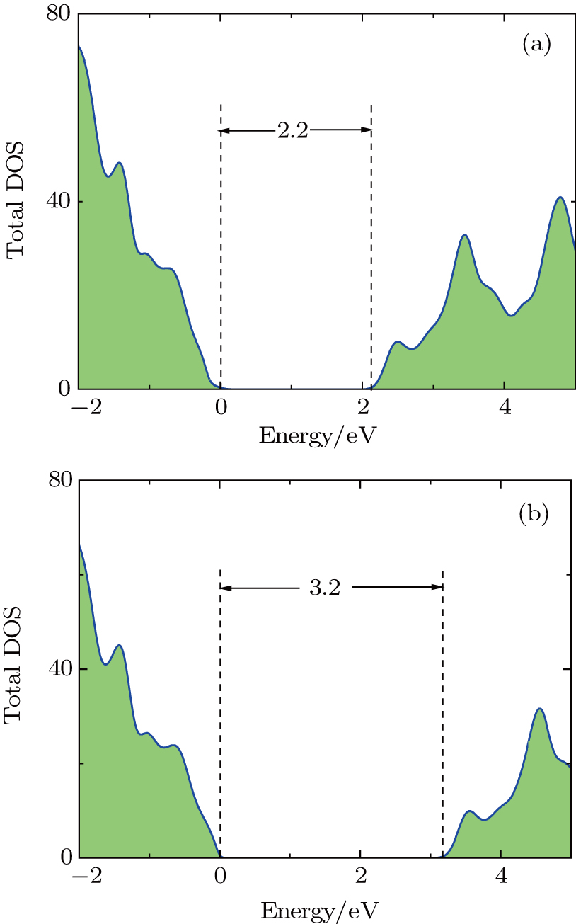
The standard DFT and the HSE06 hybrid functional scheme were employed to calculate the DOS of the 4H–SiC band gap. The results showed that the standard DFT underestimated the band gap of 4H–SiC as shown in Fig. 1. Therefore, we used the HSE06 hybrid functional scheme for calculating the DOS[3941] to obtain the relevant data close to the experimental values.

Fig. 1. (color online) DOSs of 4H–SiC calculated (a) by standard DFT, in which the band gap is 2.2 eV, and (b) by HSE06 hybrid function, in which the band gap is 3.2 eV. The 4H–SiC band gap obtained in the experiment is 3.26 eV. Level of 0 eV is marked as valence band energy of SiC.
3. Results and discussion
3.1. Defect structures of carbon dimer and DOS

According to the study of Li et al.,[29] we establish the amorphous SiO2/4H–SiC interface structure as shown in Fig. 2(a). The amorphous SiO2/4H–SiC interface contains 222 atoms, including 60 carbon atoms, 72 oxygen atoms, and 90 silicon atoms. On this basis, two carbon dimer defect structures in the SiO2/SiC interface are constructed as illustrated in Figs. 2(b) and 2(c). The two carbon dimer defects replace the Si atoms at different positions of the SiO2/SiC interface, and the carbon atoms are mutually bonded into a double-bond pattern. The bond lengths are 1.34 Å and 1.35 Å, respectively. The total energy of O2–C = C–O2 is 0.13 eV lower than that of O2–(C = C)–O2. We consider that the O2–C = C–O2 defect is more favorable in energy.

Fig. 2. (color online) (a) Interface structure of amorphous SiO2/4H–SiC. (b) Interface structure of SiO2/SiC containing a carbon dimer defect, named the O2–C = C–O2 defect. (c) Another interface structure of SiO2/SiC containing a carbon dimer defect, named the O2–(C = C)–O2 defect.

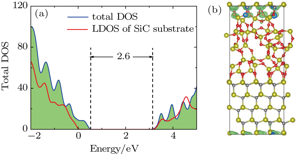
After we obtain the structural model, we calculate the DOSs for these three structures by using the HSE06 hybrid function. In Fig. 3, the band gap of the amorphous SiO2/4H–SiC interface is 2.6 eV, and some DOSs appear at the valence band maximum compared with the band gap of SiC. We calculate the partial charge density corresponding to the internal energy band in an energy level range of 0 eV–0.6 eV to investigate the cause of DOS occurrence. An energy band is determined at the energy level, and the corresponding charge density is shown in Fig. 3(b). The DOS in the energy level range of 0 eV–0.6 eV is provided by the interface between the carbon layer of SiC and that of the SiO2, instead of between the carbon dimer defects. The band gap of the amorphous SiO2/4H–SiC interface is 2.6 eV.

Fig. 3. (color online) (a) DOS in amorphous SiO2/4H–SiC interface. Maximum of valence band of the SiC substrate is set to be 0 eV. The red line represents partial density of states (PDOS) of SiC substrate, and the blue line denotes the three total DOSs of the interface structure. (b) Partial charge density diagram of energy band in amorphous SiO2/4H–SiC interface in energy level range of 0 eV–0.6 eV. Isosurface value is set to be 0.03 e/Bohr3.

Figure 4 shows the DOSs of the SiO2/SiC interface with carbon dimer defects and the partial charge density diagrams with the energy band of the interface in an energy level range of 0.6 eV–3.2 eV. The DOS diagrams shown in Figs. 4(a) and 4(b) present the defects of the carbon dimer introduced DOS in the band gap of the amorphous SiO2/4H–SiC interface. The calculation of the partial charge density indicates that the two structures with defects each contain an energy band in the energy level range of 0.6 eV–3.2 eV. The partial charge density diagrams in Figs. 4(c) and 4(d) each depict that the DIT in the band gap is provided by O2–C = C–O2 and O2–(C = C)–O2 defects. Therefore, the DOSs caused by the defects of the carbon dimers are expected to be eliminated through the passivation.

Fig. 4. (color online) DOSs of (a) O2–C = C–O2 defect and (b) O2 –O2 defect. Partial charge density diagrams of the energy band corresponding to (c) O2–C = C–O2 defect and (d) O– –O2 defect in energy level range of 0.6 eV–3.2 eV. Isosurface value is set to be 0.03 e/Bohr3.
3.2. Defect structure and DOS of carbon dimer defects after H2 passivation

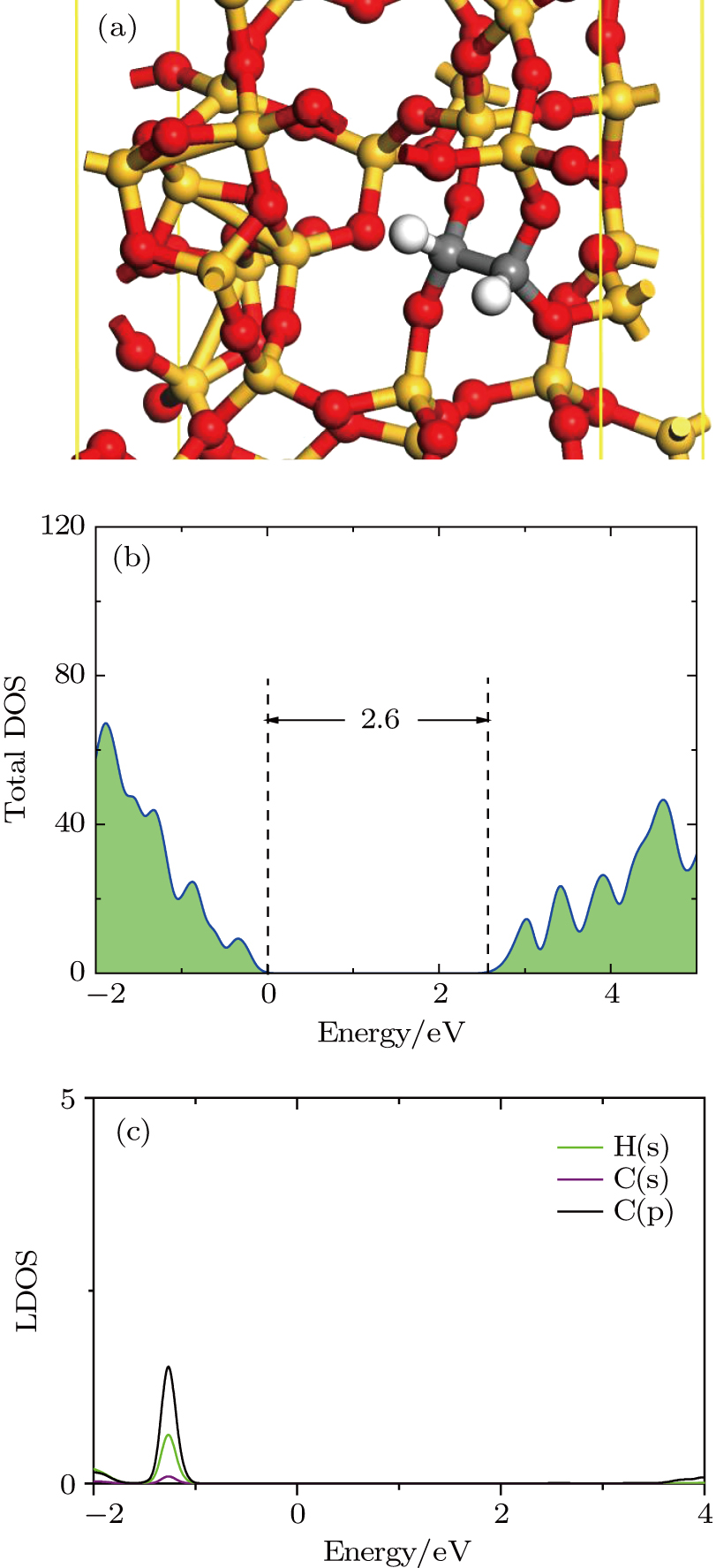
We study the carbon dimer defect structures passivated by H2. After structure optimization, we obtain the structure and its DOS as shown in Fig. 5. In Fig. 5(a), the two H atoms are adsorbed on the two C atoms of the carbon dimer and convert the carbon–carbon double bond into a single bond, the carbon–carbon bond length increases to 1.54 Å and the formation energy is −2.06 eV. Figure 5(b) demonstrates that the DOS originally distributed in the band gap is eliminated after H2 passivation. The PDOS in Fig. 5(c) illustrates that H and C atom form a hybridized peak at the valence band. So the bonding character of C–H has a bonding state. This result indicates that H2 can be adsorbed on the O2–C = C–O2 defect, thereby effectively passivating the defect. However, we cannot obtain the O2 –O2 defect structure passivated by H2. In O2–C = C–O2 defect structure after H2 passivation, C–H bond energy is 1.03 eV, and the length of C–H bond is 1.08 Å, which is in a reasonable range (about 1.09 Å). However, in O2 –O2 defect structure, the H atoms exist in the form of H2, and the distance between C and H is longer than 2.76 Å, it is far longer than the C–H bond length, the formation energy of O2 –O2+ H2 is greater than 0.54 eV. It shows that the H atoms are not adsorbed on the O2 –O2 defect. In the experimental study, the H2 annealing passivation process is controversial due to its poor effect.[22,24,25] One possible reason is that H2 cannot passivate certain types of defects, thereby failing to eliminate the DOS in the SiO2/4H–SiC band gap completely and weakening the passivation effect.

Fig. 5. (color online) (a) O2–C = C–O2 defect structure after H2 passivation, (b) its total DOS, and (c) PDOSs of atoms in the passivation region.
3.3. Defect structure and DOS of carbon dimer defects after NO passivation

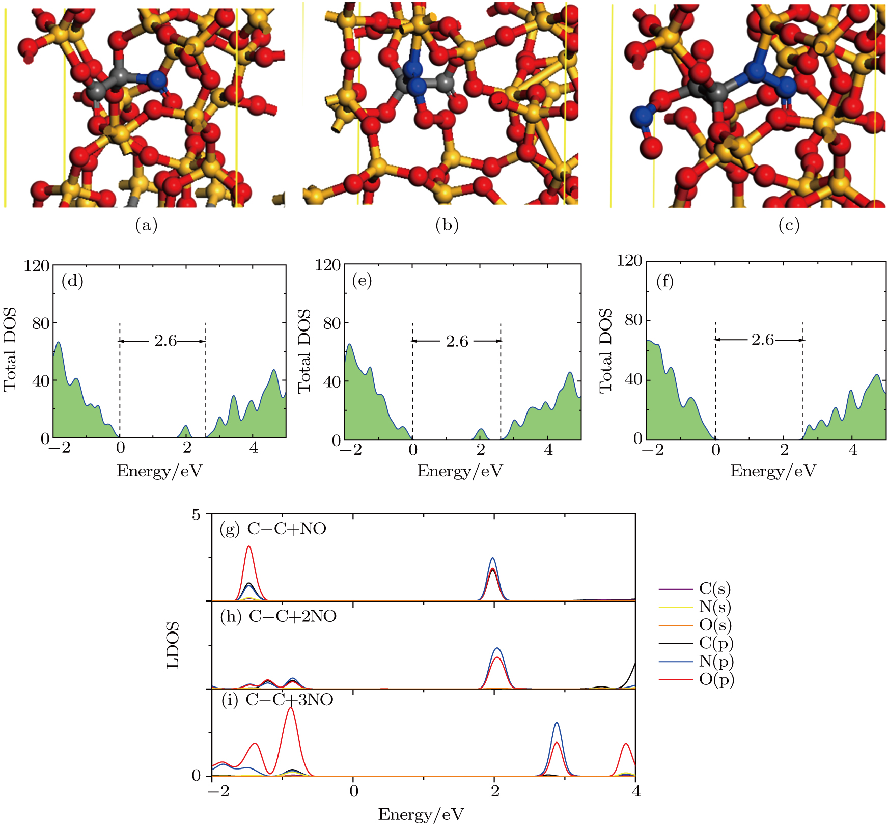
The results of O2–C = C–O2 defect after NO passivation are shown in Fig. 6. Figure 6(a) shows the O2–C = C–O2 defects of the SiO2/SiC interface by NO molecule passivation. The NO molecule is adsorbed on one of the C atoms, which leads to a carbon–carbon bond length of 1.46 Å and a formation energy of −2.81 eV. The carbon–carbon double bond is finally transformed and the O = C–C–NO structure is formed. The total DOS diagram shown in Fig. 6(d) shows that DOS remains in the band gap. The PDOSs of C, N, and O atoms are displayed in Fig. 6(g), the hybridized peaks are distributed in the valence band and band gap, indicating that the bonds of C, N, O have both bonding and antibonding states. The graphs of DOS show that an NO molecule cannot effectively passivate the O2–C = C–O2 defect, and this defect structure is required for further passivation. Figure 6(b) shows the defect structure after further passivation. In the C–C + 2NO structure, two N atoms are connected, the carbon–carbon bond length is 1.56 Å and the formation energy is −3.18 eV. The O = C–C–NO structure passivated by one NO molecule is subsequently transformed into an O = C–C–N2 structure, which is also connected with the O–O bond. Figure 6(e) shows that the C–C + 2NO passivation structure still contributes to the DOS in the band gap. The PDOS shown in Fig. 6(h) indicates that only N and O atoms have hybridized peaks in the band gap, the hybridized peaks relating to C atoms are only distributed by the valence band. The phenomenon exhibits that there exist only bonding states between C atom and N atom, and between C atom and O atom, while the bonds of N–O have antibonding states, and DOS in the band gap is also contributed by N–O bonds. Figure 6(c) shows the C–C + 3NO passivation structure, which is formed after introducing the third NO molecule. The NO molecule is connected to another C atom, the carbon–carbon bond length is still 1.56 Å and the formation energy is −4.76 eV. The carbon–oxygen double bond in the defective structure is converted, and the C atoms and other atoms in the entire defect structure are connected by single bonds. The total DOS diagram shown in Fig. 6(f) demonstrates that the total DOS in the band gap is eliminated and that the band gap width is 2.6 eV, which is the same as the band gap in the amorphous SiO2/4H–SiC interface. The hybridized peak of N and O atoms as shown in Fig. 6(i) shifts into the conduction band. The C atoms still have a hybridized peak in the valence band with N and O atoms. The bonding character of C–C + 3NO is similar to that of C–C + 2NO, but the antibonding states of the N–O shift from the band gap. It explains that the C–C + 3NO eliminates the density of defect states caused by the O2–C = C–O2 defect. The structural diagram of the O2–C = C–O2 defect after NO passivation presents that the O = C–C structure that appears in the first two structures without complete passivation might be an intermediate structure, which is introduced into the band gap as DOS. In the C–C + 3NO structure, C and C are connected by a single bond, the double bond of carbon–oxygen is transformed, and a better passivation effect is obtained.

Fig. 6. (color online) Structure diagrams and DOSs of the O2–C = C–O2 defect after NO passivation, showing passivation structures of (a) C–C + NO, (b) C–C + 2NO, and (c) C–C + 3NO, total DOSs of (d) C–C + NO, (e) C–C + 2NO, and (f) C–C + 3NO passivation structures, PDOSs of atoms in the passivation region of (g) C–C + NO, (h) C–C + 2NO, and (i) C–C + 3NO passivation structures.

The results of the O2–(C = C)–O2 defect after NO passivation are shown in Fig. 7. The + NO–I structure in Fig. 7(a) shows that the N and O atoms of the NO molecule are connected to two C atoms and that the carbon–carbon bond length is 1.55 Å and the formation energy of passivation is −2.30 eV. In this structure, the carbon–carbon double bond is converted. However, the total DOS in Fig. 7(c) shows that the structure does not eliminate the DOS in the band gap. Figure 7(e) demonstrates that the C, N, and O atoms have two hybridized peaks in the valence band, but the hybridized peak in the band gap is only contributed by N and O atoms. The condition shows that C has only bonding states, while N–O has bonding states and antibonding states. The OC–CN ring structure might also be a defect structure, which is introduced as DOS in the band gap. After adding a second NO, we obtain + 2NO–I as shown in Fig. 7(b). In this structure, two C atoms are separated and the formation energy is −6.00 eV, thereby forming the structures of O2C = CO and O2C = CN. The total DOS diagram in Fig. 7(d) shows that the DOS in the band gap is eliminated and the band gap is 2.6 eV, indicating that + 2NO–I is a completely passivated structure. The PDOSs of C, N, and O as observed in Fig. 7(f) have hybridized peaks in the valence band and conduction band, illustrating that the bonds of the C, N, and O atoms have bonding states and antibonding states, and have no DOS in the band gap. In a word, the two structures, O2C = CO and O2C = CN, do not produce DOS in the band gap.

Fig. 7. (color online) Structure diagrams and DOSs of the O2 –O2 defect after NO passivation, showing passivation structures of (a) + NO–I, and (b) + 2NO–I, total DOSs corresponding to (c) + NO–I and (d) + 2NO–I, PDOSs of atoms in the passivation region of (e) + NO–I and (f) + 2NO–I.

For further calculations, we obtain another type of NO passivation O2 –O2 defect structure. The result is shown in Fig. 8. In Fig. 8(a), the NO is connected to one of the C atoms in the + NO–II structure, the O = C–C–NO structure is generated, the carbon–carbon bond length is 1.45 Å, and the formation energy is −2.47 eV. The total DOS of + NO–II is shown in Fig. 88(c). The band gap is only 1.7 eV, which is much less than 2.6 eV. The calculation results show that the DOS in the band gap is not eliminated. The DOS in the band gap is provided by C, N, and O atoms, indicated by observing the PDOS from Fig. 8(e), and they have hybridized peaks in valence band and band gap, indicating that the bonding characters of C, N, and O bonds have bonding states and antibonding states. On the basis of the + NO–II structure, we add another NO calculation to obtain +2NO–II, and the results are shown in Fig. 8(b). In this structure, the second NO molecule is connected to another C atom, thereby transforming the carbon–oxygen double bond; the carbon–carbon bond length is 1.46 Å and the formation energy is −3.70 eV. The total DOS shown in Fig. 8(d) indicates that the band gap of + 2NO–II is 2.6 eV, and the DOS in the band gap is eliminated. Therefore, + 2NO–II also has a completely passivated structure of the O2 –O2 defect. In addition, Figure 8(f) explains that the PDOSs of C–N and N–O are distributed at the valence band, respectively, which form hybridized peaks, indicating that the bonding characters of C–N and N–O both have bonding states.

Fig. 8. (color online) Structure diagrams and DOSs of the O2 –O2 defect after NO passivation, showing passivation structures of (a) + NO–II and (b) + 2NO–II, total DOSs corresponding to (c) + NO–II and (d) + 2NO–II, and PDOS of atoms in the passivation region of (e) + NO–II and (f) + 2NO–II.

The process of passivating carbon dimer defects at the SiO2/SiC interface by NO is more complicated than by H2. The key of passivating carbon dimer defects is to transform or break the carbon–carbon double bond. Moreover, the defects should be completely passivated; otherwise, some intermediate structures would also introduce DOS into the band gap.

3.4. Partial charge density of incompletely passivated interface

We calculated the partial charge densities of the four intermediate structures with incomplete passivation, namely, C–C + NO, C–C + 2NO, + NO–I, and + NO–II, to further investigate the passivation mechanism as shown in Fig. 9. After calculations, each of the four structures has an energy band in the band gap. Figure 9(a) and 9(d) show that charge distributions on the C atom occurred for C–C + NO and + NO–II, respectively, neither of which links the NO molecule, and there might exist dangling bonds on this C atom. In Fig. 9(b), the charge distribution appears in the O–O structure, indicating that the O–O structure also contributes to the DOS in the band gap. In the partial charge density diagrams as shown in Fig. 9, each N–O structure in the intermediate structure has a charge distribution. In the completely passivated structures, N–O structures also exist in C–C + 3NO and + 2NO–II but they did not introduce the DOS into the band gap. N–O structure might be affected by O = C–C and OC–CN in the intermediate structure, thereby leading to the introduction of the density of states into the band gap.

Fig. 9. (color online) Partial charge density diagrams of the intermediate structure in the band gap of SiO2/4H–SiC after incomplete passivation by NO, showing intermediate structures of (a) C–C + NO, (b) C–C + 2NO, (c) + NO–I, and (d) + NO–II. The isosurface value is set to be 0.12 e/Bohr3.
4. Conclusions

The defect structure and interface states, as well as partial charge density, in the SiO2/4H–SiC (0001) interface have been calculated and compared by using the first principle. The results show that H2 can be adsorbed on the O2–C = C–O2 defect to form a passivation structure but it has no effect on the O2 –O2 defect. The effect of H2 passivation on the SiO2/SiC interface is ineffective in an experiment, which can be explained by the H2 not being able to passivate all types of carbon dimer defects. By contrast, NO can passivate these two carbon dimer defects. A good passivation effect is achieved by connecting some of the N–C bonds. The essence of passivating carbon dimer defects in the SiO2/4H–SiC interface is that the H2 or NO molecules are adsorbed on the defect structure, thereby ultimately transforming or breaking carbon–carbon double bonds. In the passivation process, some intermediate defects are produced, such as C2NO and O = C–C, which could contribute a defective DOS in the band gap of the SiO2/4H–SiC interface. Such intermediate defects will seriously degrade the passivation quality. Therefore, the defects of the carbon dimer must be completely passivated in the passivation process to eliminate the density of defect states in the band gap completely.

Reference
[1] Casady J Johnson R W 1996 Solid State Electron. 39 1409
[2] Saddow S E Agarwal A K 2004 Advances in silicon carbide processing and applications Boston Artech House 10 11
[3] Yoder M N 1996 IEEE Trans. Electron Dev. 43 1633
[4] Lelis A J Green R Habersat D B El M 2015 IEEE Trans. Electron Dev. 62 316
[5] Roccaforte F Giannazzo F Raineri V 2010 J. Phys. D: Appl. Phys. 43 223001
[6] Warren J A Riddle M E Graziano D J Das S Upadhyayula V K Masanet E Cresko J 2015 Environ. Sci. Technol. 49 10294
[7] Afanas’ev V Stesmans A Bassler M Pensl G Schulz M 2000 Appl. Phys. Lett. 76 336
[8] Agarwal A Casady J Rowland L Valek W White M Brandt C 1997 IEEE Electron. Dev. Lett. 18 586
[9] Brown D Downey E Ghezzo M Kretchmer J Krishnamurthy V Hennessy W Michon G 1996 Solid State Electron. 39 1531
[10] Saks N Mani S Agarwal A 2000 Appl. Phys. Lett. 76 2250
[11] Spitz J Melloch M Cooper J Capano M 1998 Electron. Dev. Lett. 19 100
[12] Vathulya V R White M H 2000 Solid State Electron. 44 309
[13] Yano H Kimoto T Matsunami H 2002 Appl. Phys. Lett. 81 301
[14] Kodigala S R Chattopadhyay S Overton C Ardoin I Gordon B Johnstone D Roy D Barone D 2015 Appl. Surf. Sci. 330 465
[15] Pensl G Beljakowa S Frank T Gao K Speck F Seyller T Ley L Ciobanu F Afanasév V Stesmans A 2008 Phys. Status Solidi 245 1378
[16] Sun Q J Zhang Y M Song Q W Tang X Y Zhang Y M Li C Z Zhao Y L Zhang Y M 2017 Chin. Phys. 26 127701
[17] Li W B Li L Wang F F Zheng L Xia J H Qin F W Wang X L Li Y P Liu R Wang D J Pan Y Yang F 2017 Chin. Phys. 26 037104
[18] Yoshikawa M Saitoh K Ohshima T Itoh H Nashiyama I Yoshida S Okumura H Takahashi Y Ohnishi K 1996 J. Appl. Phys. 80 282
[19] Afanasév V Bassler M Pensl G Schulz M 1997 Phys. Status Solidi 162 321
[20] Afanasév V Ciobanu F Dimitrijev S Pensl G Stesmans A 2004 J. Phys.: Condens Matter 16 S1839
[21] Fukuda K Suzuki S Tanaka T Arai K 2000 Appl. Phys. Lett. 76 1585
[22] Cantin J L Von Bardeleben H Ke Y Devaty R Choyke W 2006 Appl. Phys. Lett. 88 092108
[23] Campi J Shi Y Luo Y Yan F Zhao J H 1999 IEEE Trans. Electron Dev. 46 511
[24] Ueno K Asai R Tsuji T 1998 Electron. Dev. Lett. 19 244
[25] Wang S Dhar S Wang S Ahyi A Franceschetti A Williams J Feldman L Pantelides S T 2007 Phys. Rev. Lett. 98 026101
[26] Chung G Tin C Williams J McDonald K Di Ventra M Pantelides S Feldman L Weller R 2000 Appl. Phys. Lett. 76 1713
[27] Knaup J M Deák P Frauenheim T Gali A Hajnal Z Choyke W 2005 Phys. Rev. 71 235321
[28] Devynck F Giustino F Pasquarello A 2005 Microelectron. Eng. 80 38
[29] Li W Zhao J Wang D 2015 Solid State Commun. 205 28
[30] Deak P Knaup J M Hornos T Thill C Gali A Frauenheim T 2007 J. Phys. D: Appl. Phys. 40 6242
[31] Devynck F Pasquarello A 2007 Phys. B Condens Matter 401 556
[32] Kresse G Furthmüller J 1996 Comp. Mater Sci. 6 15
[33] Kresse G Furthmüller J 1996 Phys. Rev. 54 11169
[34] Perdew J P Burke K Ernzerhof M 1996 Phys. Rev. Lett. 77 3865
[35] Monkhorst H J Pack J D 1976 Phys. Rev. 13 5188
[36] Alkauskas A Broqvist P Pasquarello A 2008 Phys. Rev. Lett. 101 046405
[37] Alkauskas A Broqvist P Pasquarello A 2011 Phys. Status Solidi 248 775
[38] Zhang S Tomanek D Louie S G Cohen M L Hybertsen M S 1988 Solid State Commun. 66 585
[39] Heyd J Scuseria G E Ernzerhof M 2003 J. Chem. Phys. 118 8207
[40] Krukau A V Vydrov O A Izmaylov A F Scuseria G E 2006 J. Chem. Phys. 125 224106
[41] Paier J Marsman M Hummer K Kresse G Gerber I C Ańgyań J G 2006 J. Chem. Phys. 124 154709