


Ultra-high voltage 4H-SiC gate turn-off thyristor for low switching time
Cite this Article
Liu Qing, Pu Hong-Bin, Wang Xi. Ultra-high voltage 4H-SiC gate turn-off thyristor for low switching time. Chinese Physics B, 2019, 28(12): 127201 
Permissions
Ultra-high voltage 4H-SiC gate turn-off thyristor for low switching time
† Corresponding author. E-mail:
Project supported by the National Natural Science Foundation of China (Grant No. 51677149).
Abstract
An ultra-high voltage 4H-silicon carbide (SiC) gate turn-off (GTO) thyristor for low switching time is proposed and analyzed by numerical simulation. It features a double epitaxial p-base in which an extra electrical field is induced to enhance the transportation of the electrons in the thin p-base and reduce recombination. As a result, the turn-on characteristics are improved. What is more, to obtain a low turn-off loss, an alternating p+/n+ region formed in the backside acts as the anode in the GTO thyristor. Consequently, another path formed by the reverse-biased n+–p junction accelerates the fast removal of excess electrons during turn-off. This work demonstrates that the turn-on time and turn-off time of the new structure are reduced to 37 ns and 783.1 ns, respectively, under a bus voltage of 8000 V and load current of 100 A/cm2.
1. Introduction
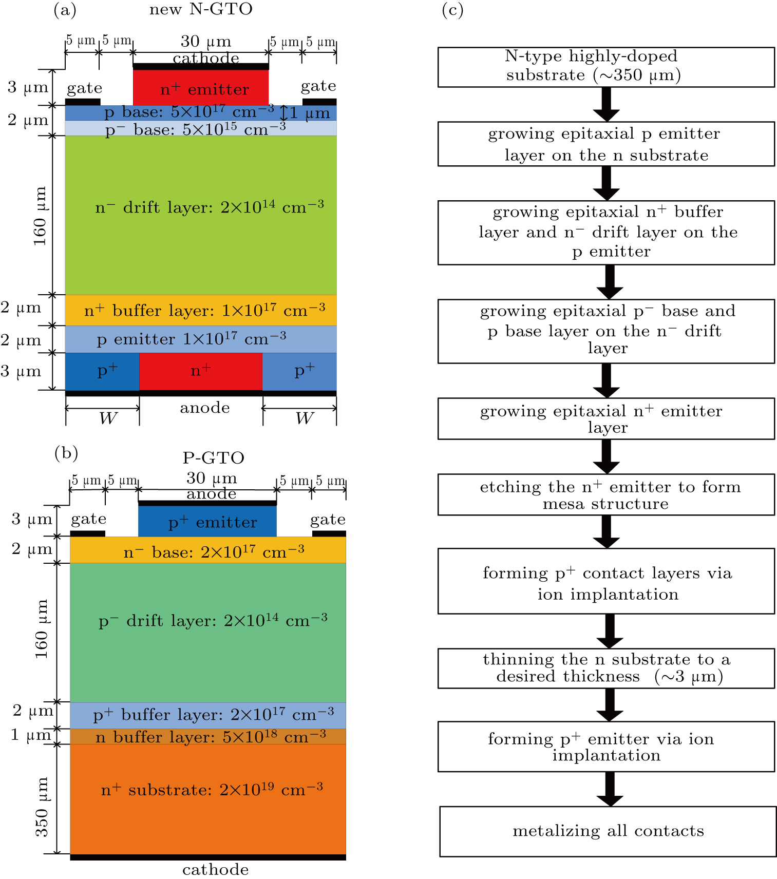
In recent years, global demand of high voltage power semiconductor devices has been increasing in many industrial fields. In particular, high voltage gate turn-off (GTO) thyristor based on SiC has rapidly developed in simulations and experiments for being used as the ultra-high voltage direct current (UHVDC) converters. The SiC GTO thyristors can withstand higher blocking voltage, operate at higher junction temperature and have faster switching speed than Si thyristor,[1,2] because SiC material has characteristics of wide bandgap, high breakdown electric field, high thermal conductivity, and radiation-resistance.[3,4] Currently, the asymmetrical 22-kV 4H-SiC GTO thyristor with a thickness of 160-μm p− drift layer is reported by Cree, Inc.[5] In fact, the development of SiC GTO thyristor with n-type drift layer is ahead of that of SiC GTO thyristor with p-type drift layer. Owing to the limitation of technology level, the SiC GTO thyristors with n-type thyristor use p-type SiC substrates that will induce a high resistance connected in series with the devices. Hence, the SiC GTO thyristor with p-type drift layer has been reported and investigated most during the past three decades. However, in 2015, the 27-kV/20-A 4H-SiC IGBTs with n-type drift layer was fabricated successfully on an n-type substrate and subsequently the n+ substrate was removed by mechanical grinding or chemical mechanical polishing (CMP).[6] Additionally, in 2017, a low cost substrate removal process was developed commercially to obtain lightly doped free standing epitaxial SiC wafers with atomically flat surfaces on both Si- and C-faces. Using this process, a 350-μm-thick n+-SiC substrate has been successfully removed to fabricate 180-μm–250-μm-thick 4-inch-sized (1 inch = 2.54 cm) n-SiC epitaxial free standing wafers by electrochemical etching process.[7] Hence, the fabrication of the SiC thyristors with thick n-type drift layer is feasible. Besides, n-type GTO thyristors have a high upper transistor gain αNPN (∼ 0.95) due to the strong electron injection from the upper n+ emitter. What is more, the n-type GTO thyristors have a small lower transistor gain αPNP (∼ 0.05–0.2) caused by the low hole injection from the bottom p+ emitter.[8] Thus, the turn-on and turn-off characteristics of n-type GTO thyristor are ferior to those of p-type GTO thyristor.
In our previous work, a double epitaxial n-base in p-type SiC thyristors[9] is induced to reduce the turn-on time. But unfortunately, the turn-off time of the thyristor is increased. In view of this, we consult the method to gain low turn-off loss in Si thyristor by the anode- or cathode-shorts[10,11] to improve the turn-off characteristics in SiC thyristors.
In this paper, an ultra-high voltage 4H-SiC GTO thyristor with n− drift layer for low switching time is proposed and demonstrated by numerical simulations, which shows excellent turn-on and turn-off performance.
2. Device structure and simulation setup
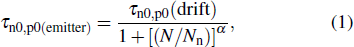
where τn,p(drift) are the values of the parameters τn and τp0 in the thick n−/p− drift layer, N is the doping concentration for the heavily doped emitters, and Nn and α are the fitting parameters, Nn = 7 × 1017 cm−3, and α = 1. Table 1 shows several important physical models and their parameters in this simulation. Moreover, all simulations are carried out by using Fermi–Dirac statistics. The temperature involved in all simulations is assumed to be room temperature (300 K). Moreover, in the simulation, the minority carrier lifetime in the drift layer and buffer layer are set to be 2.0 μs and 1.5 μs, respectively.[23]
Figure
 | Fig. 1. Cross-sectional schematic diagram of (a) proposed 4H-SiC n-GTO thyristor, (b) conventional p-GTO thyristor, and (c) simple fabrication process of proposed n-GTO thyristor. |
Figure
Figure
To investigate the static and dynamic characteristics of the developed n-type GTO thyristor, two-dimensional device-level simulation software Sentaurus-TCAD[15] is used. In simulations, some models must be adopted, including incomplete ionization,[16] band-gap narrowing,[17] Auger recombination,[18] electron–hole scattering,[19] doping, temperature, and field-dependent mobility models,[20] Shockley–Read–Hall recombination with the Scharfetter.[21] For impact-ionization modeling, the anisotropic model is used for the SiC-based GTO thyristor.[22] In the highly-doped p+/n+ emitter layers, the carrier lifetime is given by the semi-empirical formula[23,24]
 |
| Table 1. Physical models and parameters. . |
3. Results and discussion
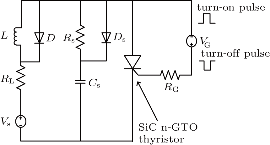
In this section, we will investigate the static and dynamic characteristics for the SiC GTO thyristors comparatively. The results and analyses are presented as follows. Also the device active area is taken to be 1 cm2 for simplicity. The test circuit as shown in Fig.
 | Fig. 2. Test circuit of dynamic characteristics of 4H-SiC GTO thyristor. |
Figures
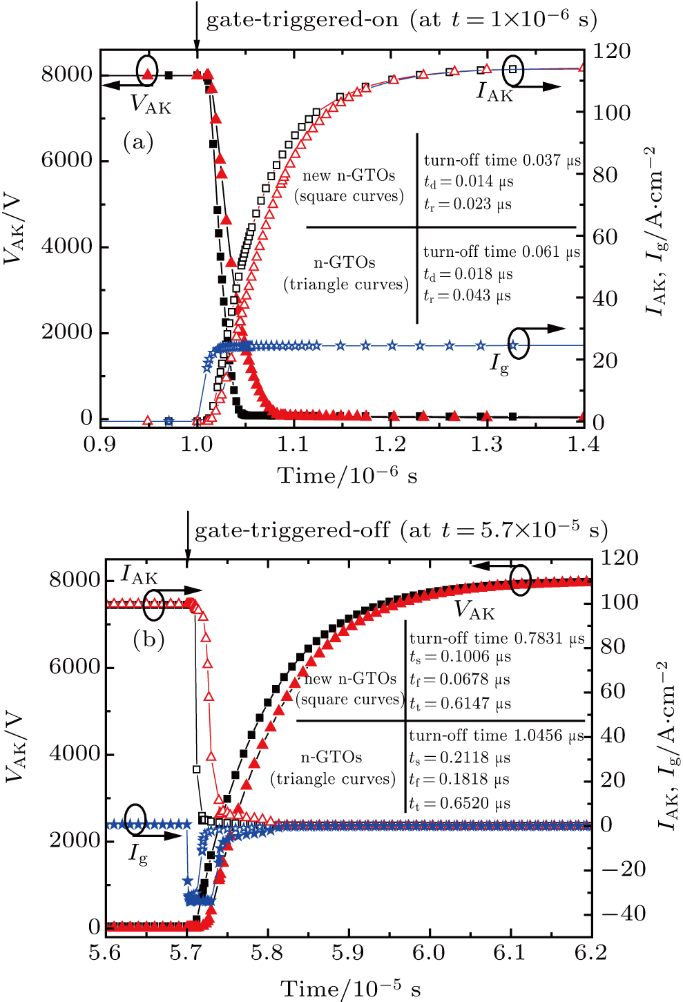
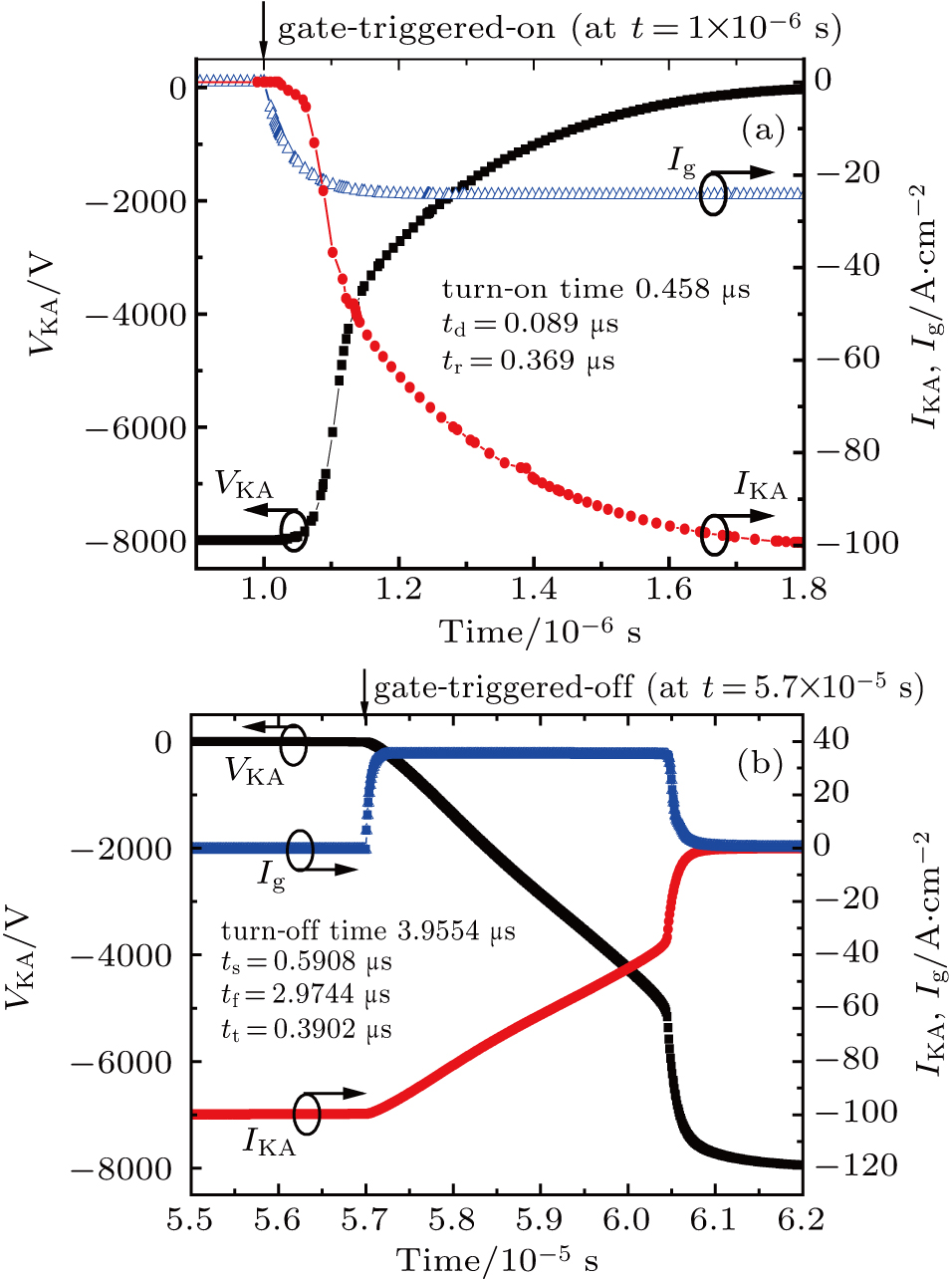
 | Fig. 3. Switching waveforms of proposed n-GTO and n-GTO thyristors for (a) turn-on case and (b) turn-off case. |
 | Fig. 4. Switching waveforms of p-GTO thyristors for (a) turn-on case and (b) turn-off case. |
Results show that comparing with the p-type GTO, the turn-on time and turn-off time of the n-type GTO decrease extremely, which can be explained by the higher injection efficiency of the top n+–p junction and the smaller transistor current gain of the bottom p–n–p transistor of the n-type GTO than those of p-type GTO. Hence, the switching performance of the n-type GTO is superior to p-type GTO.
Besides the dynamic characteristics of the structures, the forward on-state characteristics of the developed SiC GTO thyristors are also presented as follows.
Figure
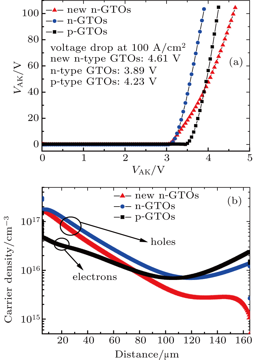
 | Fig. 5. (a) Forward J–V characteristics of structures, and (b) distribution of holes/electrons in n/p drift layer at on-state current density of 100 A/cm2. |
The comparison between the dynamic performance and the static performance given above shows that the switching characteristics of the proposed 4H-SiC n-type GTO thyristor is improved significantly at the sacrifice of a little on-state performance. Subsequently, the turn-on and turn-off mechanisms of the new n-type GTO thyritsor are investigated in detail.
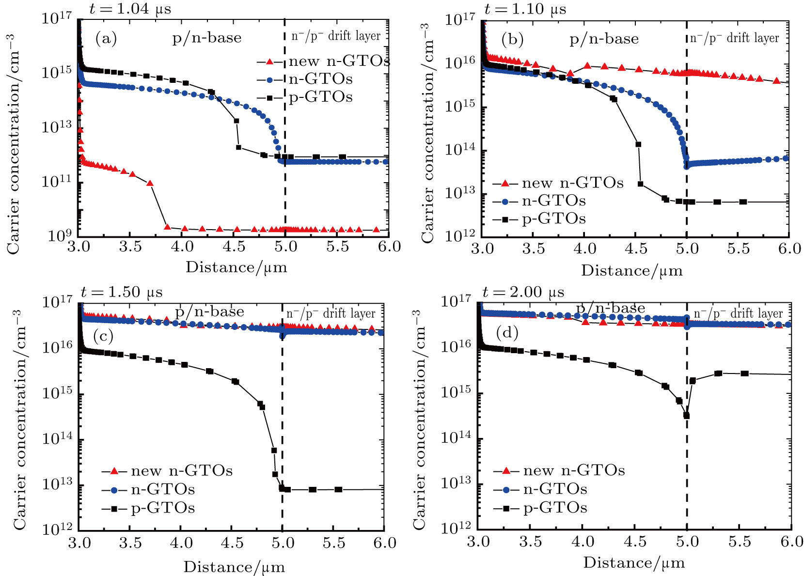
3.1. Analysis of turn-on mechanism
As can be seen from the results of Fig.
 | Fig. 6. Plots of minority carrier (electron/hole) density versus distance in thin p-base/n-base of SiC GTO thyristors in turn-on process. |
Figure
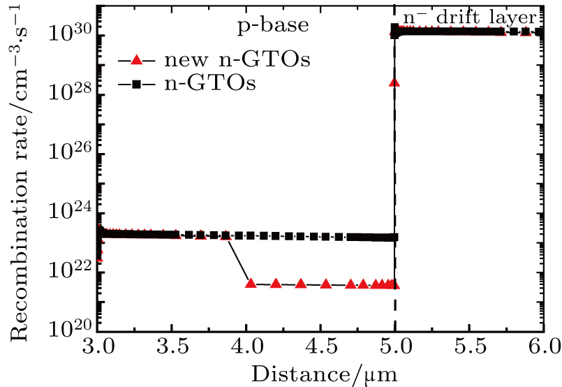 | Fig. 7. Recombination rate versus distance of two n-type GTO thyristors during turn-on state. |
3.2. Analysis of turn-off mechanism
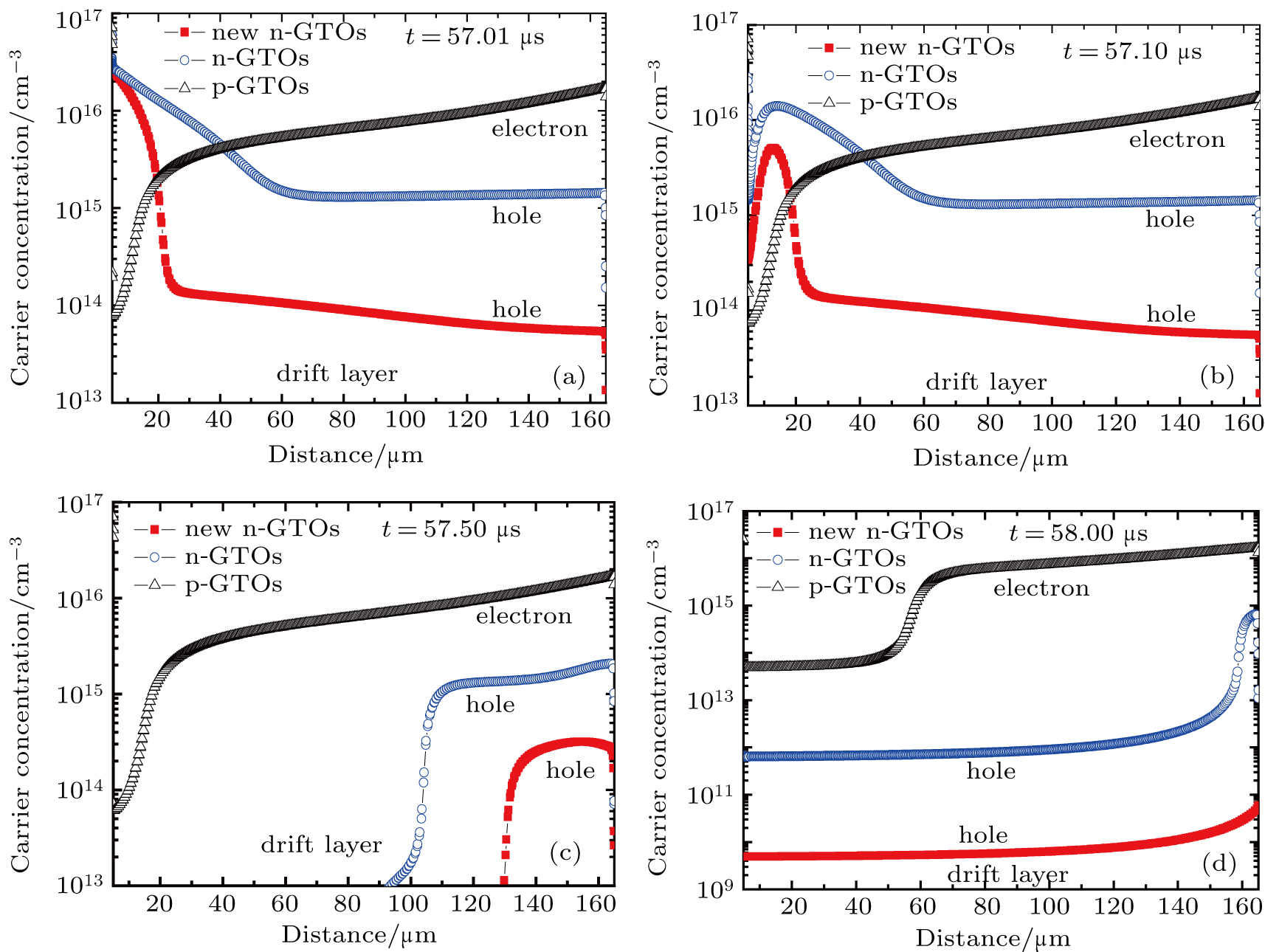
The dynamic turn-off characteristics of the structures, which are obtained with a 33-A/cm2 absolute value of gate current (the turn-off gain βoff ≈ 3), are shown in Figs.
Figure
 | Fig. 8. Minority carrier concentration distributions at different times during turn-off state. |
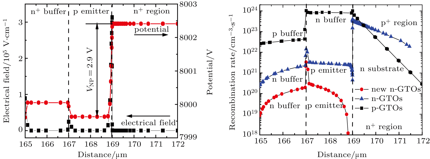 | Fig. 9. (a) Electrical field distribution in new 4H-SiC GTO thyristor and (b) recombination rate distribution during turn-off state for different structures. |
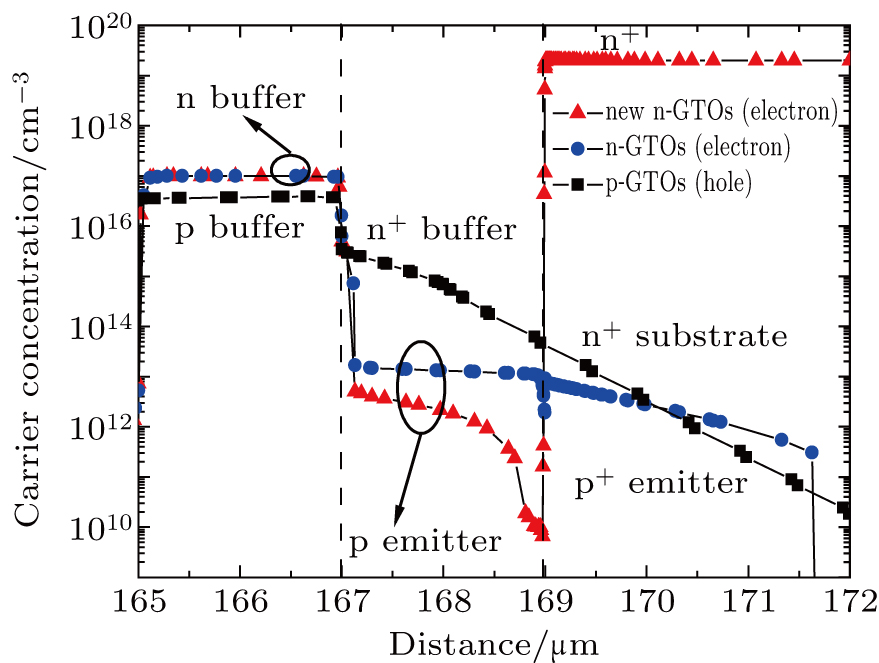 | Fig. 10. Carrier density distributions during turn-off state for different structures. |
Figure
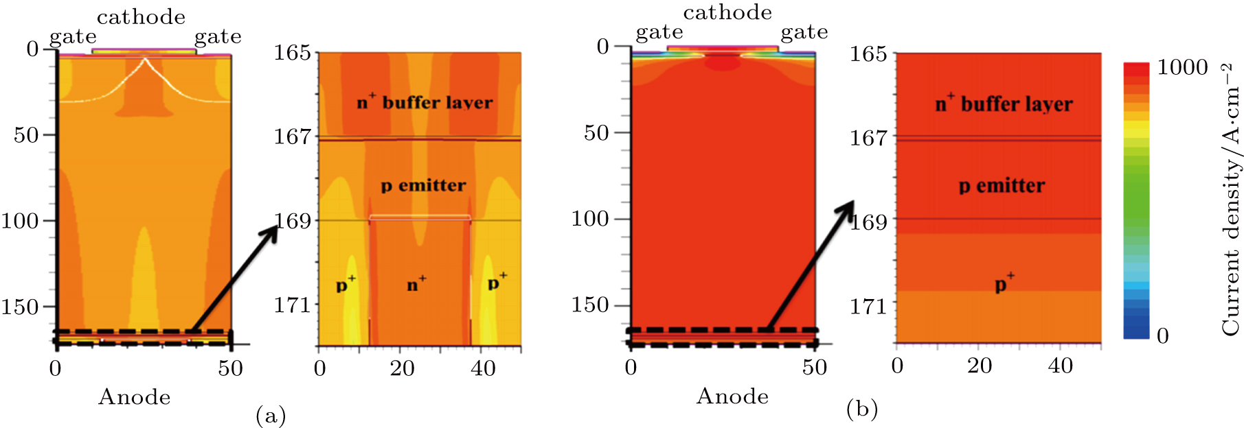
 | Fig. 11. Current density distribution during turn-off state in (a) new n-GTO thyristor and (b) conventional n-GTO thyristor. |
4. Conclusions and perspectives
In this paper, a novel ultra-high voltage 4H-SiC GTO thyristor for low switching loss is presented. The results demonstrate that for the proposed 20-kV n-type 4H-SiC GTO thyristor, the turn-on time and turn-off time are reduced to 37 ns and 783.1 ns, respectively. During turn-on state, the extra electric field introduced by the high–low p–p− junction in the thin p-base enhances the transit of the electrons and reduces the recombination. During the turn-off state, the outstanding turn-off characteristics are attributed to the following two aspects. First, the extra carriers in an n− drift layer are less during the turn-on state in the new n-type GTO thyristor. Second, and most important thing of all, during the turn-off state, is that the bottom n+–p junction is reverse-biased, which accelerates the extraction of electrons. As a result, the turn-on and turn-off characteristics of the proposed structure are improved significantly with a slight degradation of the forward voltage drop. The idea can be a promising solution for fast switching the ultra-high voltage SiC GTO thyristor.
Reference
| [1] | |
| [2] | |
| [3] | |
| [4] | |
| [5] | |
| [6] | |
| [7] | |
| [8] | |
| [9] | |
| [10] | |
| [11] | |
| [12] | |
| [13] | |
| [14] | |
| [15] | |
| [16] | |
| [17] | |
| [18] | |
| [19] | |
| [20] | |
| [21] | |
| [22] | |
| [23] | |
| [24] | |
| [25] |