Defects and electrical properties in Al-implanted 4H-SiC after activation annealing
Tang Yi-Dan1, 2, †, Liu Xin-Yu1, ‡, Zhou Zheng-Dong3, Bai Yun1, Li Cheng-Zhan3
High-Frequency High-Voltage Devices and Integrated Circuits Research and Development Center, Institute of Microelectronics of Chinese Academy of Sciences, Beijing 100029, China
University of Chinese Academy of Sciences, Beijing 100049, China
Zhuzhou CRRC Times Electric Co., Ltd, Zhuzhou 412001, China


† Corresponding author. E-mail: tangyidan@ime.ac.cn xyliu@ime.ac.cn

Abstract

The defects and electrical properties in Al-implanted 4H-SiC after activation annealing (1600 °C–1800 °C) are investigated. High temperature annealing can reduce the ion implantation-induced damage effectively, but it may induce extended defects as well, which are investigated by using Rutherford backscattering spectroscopy (RBS/C), secondary ion mass spectroscopy (SIMS), and transmission electron microscopy (TEM) analyses. According to the ratio of the channeled intensity to the random intensity in the region just below the surface scattering peak (Xmin) and RBS/C analysis results, the ion implantation-induced surface damages can be effectively reduced by annealing at temperatures higher than 1700 °C, while the defects near the bottom of the ion-implanted layer cannot be completely annealed out by high temperature and long time annealing process, which is also demonstrated by SIMS and TEM analyses. Referring to the defect model and TEM analyses, an optimized annealing condition can be achieved through balancing the generation and elimination of carbon vacancies in the ion implanted layers. Furthermore, the electrical and surface properties are also analyzed, and the hole concentration, mobility, and resistivity are obtained through the Hall effect. The optimized activation annealing conditions of 1800 °C/5 min are achieved, under which the lower defects and acceptable electrical properties are obtained.

1. Introduction

Semiconductor material, SiC, is attractive for the applications in high power, high temperature, high frequency, and high reliability device due to its exceptional properties.[18] P-type doping of 4H-SiC using ion implantation and high temperature activation annealing is the key process in the fabrication of SiC devices.[2,3] Compared with boron (B), aluminum (Al) has a shallow acceptor level and a strong tendency to occupy atomic sites in the silicon (Si) sublattice, which makes Al+ ion implantation more suitable for the production of heavily doped layers.[914] However, a great challenge exists in the effective doping of Al, because high energy of Al ion implantation inevitably produces defects and lattice disorder. Although redistribution of the implanted dopants and partial ion-induced damages can be reduced by high temperature implantation followed by high temperature annealing, not all the damages could be annealed out by higher temperature annealing, such as residual damages (distortion of lattice, vacancies and interstitials) and extended defects, because of dynamic defect recovery and generation in the activation annealing process.[1326] And it was reported that the formation of extended defects in the implanted layers and the interfacial dislocations of the ion-implanted layer can occur in the annealing process.[15,20,23] Such high residual damages and extended defects of the implanted layers will greatly affect the electrical performance and reliability of SiC device, such as the mobility in MOSFETs and leakage current in PIN diodes. How to suppress the generation and distribution of these defects is still an open issue in the study of this subject. Therefore, a clearer understanding of the recovery, formation and distribution of the defects in the Al-implanted layers during the implantation and annealing processing is beneficial to obtaining the better electrical properties in Al-implanted 4H-SiC through optimization of activation annealing conditions.

In this paper, the defects and electrical properties in Al-implanted 4H-SiC after high-temperature activation annealing (1600 °C–1800 °C) are investigated. The ion implantation-induced damages and the extended defects after the annealing process are investigated by using Rutherford backscattering spectroscopy (RBS/C), secondary ion mass spectroscopy (SIMS), transmission electron microscopy (TEM) analyses. The optimized activation annealing conditions are achieved, under which the lower defects and acceptable electrical properties are achieved and demonstrated by the Hall effect measurement.

2. Experiment

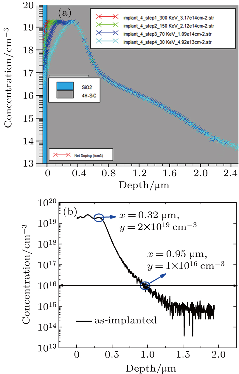
Multiple-energy Al implantations were performed on n-type, 4° off the (0001) oriented 4H-SiC epilayer at a doping concentration of 1×1016 cm−3. Hot implantation (500 °C) was used to hinder amorphization and improve the quality of crystalline in Al-implanted 4H-SiC. As seen from Fig. 1(a), the implantation at energy ranging from 30 keV to 300 keV with a total dose of 8.41×1014 cm−2 formed a box-like doping profile with a 6-nm-thick sacrificial oxidation silicon dioxide (SiO2) layer. And the obtained doping concentration of with a depth of about 320 nm after removing a 60-nm-thick sacrificial oxidation SiO2 layer was characterized by SIMS measurement as shown in Fig. 1(b).

Fig. 1. (a) Simulated concentration versus depth profiles of Al atoms after multiple energy implantations into SiC with the purpose of forming a box-like profile by using the Silvaco TCAD, and (b) doping concentration profiles measured by SIMS after removing 60-nm-thick sacrificial oxidation SiO2 layer.

Post-implantation annealing was processed at 1600 °C–1800 °C with a protective carbon capping layer. Effects on Al ion implantation on n-type 4H-SiC followed by annealing at various temperatures was studied by using RBS/C, SIMS, TEM, and atomic force microscope (AFM) analyses. Transmission line model (TLM) and Hall effect measurements are also conducted to analyze the electrical properties.

3. Results and discussion
3.1. Defects analysis

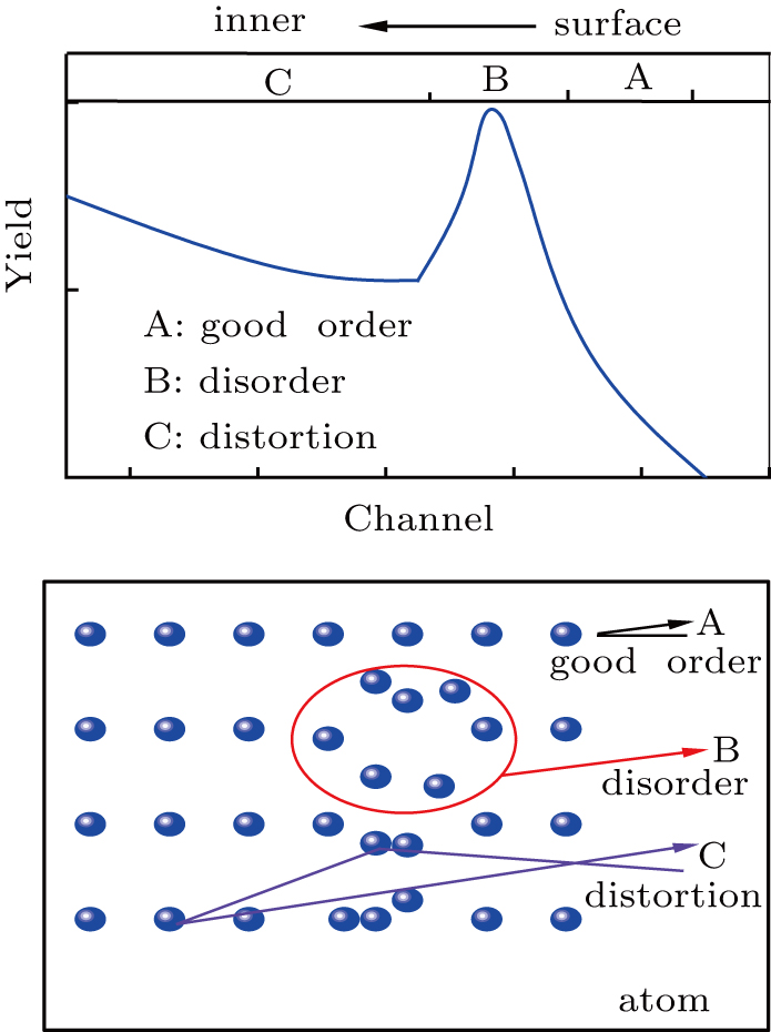
As one of the most common surface analytical techniques, Rutherford backscattering spectrometry along a low index crystallographic direction or channel (RBS/C) is sensitive to very small atomic displacements from the crystalline lattice sites. The RBS/C interaction yield is strongly influenced by the crystal disorder and crystal orientation, which makes the technique unique for the analysis of ion implantation damage in single-crystal films and wafers. As shown in Fig. 2, A, B, and C represent three relationships between location and the status of damages with the RBS/C from surface to inner region. The energy of backscattering atoms of A have little energy loss and most of ion-beams can be channeled, indicating A is near the surface and has good order lattice. B has an obvious peak, which indicates that many dislocation atoms or disorder lattices exist under the surface; C is the inner part of the crystal, which contains the damage status of C and the effect of B. The high yield in C is mainly due to a mass of dislocation atoms, containing the distortion lattice of C and the little random atoms of B.

Fig. 2. Relationship between the location and the status of damages with RBS/C.

The Xmin refers to the ratio of the channeled intensity to the random intensity in the region just below the surface scattering peak. It yields information about the crystallinity in the near surface of the sample (the first 3 nm–15 nm in depth), which is related to the surface damage, contamination and the existence of oxides. Figure 3 shows the Xmin values of samples before and after thermal implantation annealing at various temperatures (1600 °C–1800 °C) for 15 min. Each of all the annealed samples has a smaller Xmin value than that of the as-implanted (Xmin =0.403) and the Xmin value decreases with annealing temperature rising up. With the annealing temperature higher than 1700 °C, the sample’s surface damage can be effectively reduced.
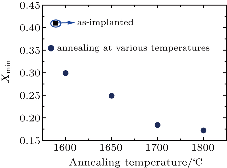
Fig. 3. Variation of Xmin (160° detector ) with temperature of implanted samples before and after activation annealing for 15 min.

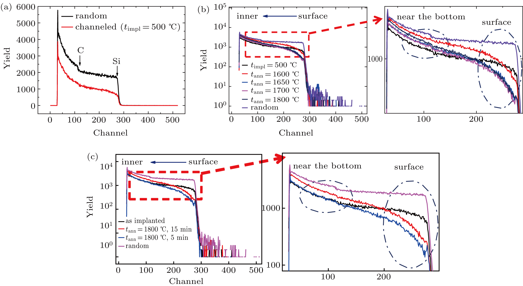
From Figs. 4(a)4(c), all the samples of SiC samples can be channeled, and the channeling yield increases with channel number decreasing without obvious damage peaks, which do not reach the random level. The crystal has no obvious amorphous layer and the experimentally obtained RBS spectra after annealing are closely identical to the fresh virgin spectrum. It can be concluded that the use of hot temperature (500 °C) implantation can avoid forming the high-density extended defects, dopant redistribution, and surface decomposition in the implanted layer. However, corresponding to the random spectra, a defective layer containing a low level of lattice displacement or distortion is formed on the implanted sample in Fig. 4(a).

Fig. 4. Overlays of implanted samples (a) before and (b) after activation annealing at various temperatures for 15 min and (c) at 1800 °C and different annealing times.

In the amplified regions on the right in Figs. 4(b) and 4(c), the densities of defects near surface under all the annealing conditions except for the sample of 1600 °C for 15 min, are lower than that of the as-implanted one, which proves that the defects near-surface region are greatly affected by annealing temperature. However, for the annealing time of 15 min, the defects near the bottom of the ion-implanted layer for each of all annealing samples are more than those of as-implanted sample at the different temperatures (from 1600 °C–1800 °C), indicated by the through RBS/C analysis results as shown in Fig. 4(b).

In order to reduce the defects both near the surface and bottom of the ion-implanted layer in high temperature annealing process, the annealing is carried under the conditions of 1800 °C for 5 min and 15 min. It is shown in the amplified region on the right in Fig. 4(c) that the damages near the surface and the bottom of the sample annealed for 1800 °C and 15 min are more pronounced than for 1800 °C and 5 min. Furthermore, as seen in Fig. 4(c), the density of defects near the bottom region under the annealing condition of 1800 °C for 15 min is higher than that of the as-implanted one, but not under the condition of 1800 °C and 5 min. It may be because the longer time thermal annealing induces new extended defects near the bottom of the ion-implanted layers. Therefore, the annealing time is another key factor affecting the generation of extended defects.

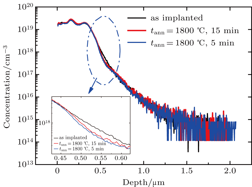
In Fig. 5, all samples are tested after removing protective carbon capping layer and sacrificial oxidation. Profiles of implanted atoms before and after annealing at 1800 °C, 15 min, and 5 min by SIMS do not coincide with each other near the bottom of the ion-implanted layer. Possible reasons are that the defect agglomeration and dopant redistribution occur near the bottom of the ion-implanted layer in the annealing process. This is consistent with the conclusion that the defects near the bottom of the ion-implanted layer will be dynamically restored and generated in the activation annealing process. Therefore, it is necessary to optimize the annealing conditions to minimize the defects near the bottom of the ion-implanted layer. As shown in the amplified area of Fig. 5, the curve of the sample obtained under the activation annealing condition (1800 °C/5 min) is highly coincident with that near the bottom of the as-implanted sample.

Fig. 5. Profiles of implanted atoms before and after annealing at 1800 °C, 15 min/5 min by SIMS after removing protective carbon capping layer and 60-nm-thick sacrificial oxidation SiO2 layer.

From the above results of the RBS-C technique, we find quite a low level of the residual disorders and extended defects in the implanted and annealed SiC layers. As a complement to RBS/C, cross section samples in the implanted region are prepared. And the lattice structure of the implanted layer and the annealed layerare also measured with TEM, which is equipped with an FEI Talos F200 transmission electron microscope at 200 kV. The samples for TEM are cross-sectioned, prepared by focused ion beam (FIB).

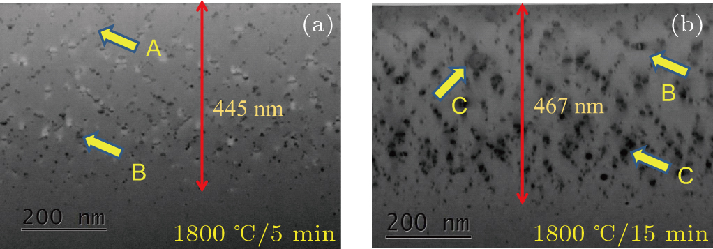
Figure 6(a) and 6(b) show cross-sectional bright field-electron (BF) micrographs of identically Al-implanted samples with the annealing temperature at 1800 °C for 15 min and 5 min, respectively. As seen from Figs. 6(a) and 6(b), the visible depths of the damage areas are 445 nm and 467 nm respectively. From the above SIMS test data, it can be inferred that the damage areas include ion implantation region and part of trailing region. In Fig. 6, all of the extended defects are visible in the Al-implanted region after 1800 °C/5 min annealing and 1800 °C/15 min annealing, especially near the bottom of Al-implanted region. These defects are lettered from A to C, which are polygonal loops differing in size. These loops form a network of almost orthogonal trace. Defect A is smallest, next is defect B. In the case of defect C, it is possible to demonstrate that it has a complex structure related to dislocations or carbon vacancy agglomerates.[1924] The distribution of these defects is not uniform and appears to peak in a buried region close to the end of the Al-implanted region, which is between the bottom of implanted Al region and the unimplanted substrate. The defects of 1800 °C/15 min sample (Fig. 6(a)) are obviously more than those of the sample with 1800 °C/5 min (Fig. 6(b)). This indicates that the longer annealing time will lead to more extended defects at the same temperature, which is in good agreement with the RBS analysis results. As shown in the amplified defects area in Figs. 7(b) and 7(c), there are many polygonal dislocation loops with different sizes. The micrograph indicates that most of the defects at the bottom of implanted Al layers created during annealing are dislocations as indicated by arrows in Fig. 7(c). The formation of these dislocations may be related to a cluster of C-related defects, such as carbon vacancies.[1926]

Fig. 6. Cross-sectional micrograph in Al-implanted region by (a) 1800 °C/5 min annealing and (b) 1800 °C/15 min annealing.
Fig. 7. Cross-sectional micrograph in Al-implanted region by 1800 °C/5 min annealing.

To obtain the mechanisms responsible for the formation and elimination of extended defects, according to the previous defect theory,[15,2123] the defect model in Al-implanted 4H-SiC layer is also investigated. The high temperature activation annealing is the process of replacing the implanted Al atoms with Si. During the activation annealing, most of dopants are activated, and the ion-induced damages are recovered because of the recrystallization of the annealed samples. As seen from Fig. 8, in the high temperature activation annealing process, the persistent carbon vacancies in the drift layers after epitaxy can be effectively recombined by the excess carbon interstitials Ci created by implation. At the same time, new carbon vacancies will be formed in the high temperature process. So, the optimization of annealing conditions can be realized by controlling the generation and elimination of carbon vacancy (VC) density in the ion implanted layers.

Fig. 8. Defect model in Al-implanted 4H-SiC layer.
3.2. Electrical and surface property analysis

As seen from Table 1, the Hall hole density P, Hall mobility μ and electrical activation ratio A ( )are improved by increasing annealing temperature through using Pensl et al.’s Hall scattering factor. Sheet resistance R and specific contact resistance (SCR) decrease with annealing temperature increasing. As the temperature increases, the rate of annealing activation increases. At the same annealing temperature, the longer time annealing can improve the electrical activation properties effectively. However, the consideration of the lower defects, the sample annealed at 1800 °C/5 min shows relatively good electrical properties.

Table 1.

Values obtained by Hall-effect and TLM measurements for p-type 4H-SiC samples at room temperature (RT).

.

Furthermore, the surface roughness values of Al-implanted samples before and after activation annealing at various temperatures are measured by AFM. We use the 5-point average of the large area implantation and activation annealing sample. The results in Table 2 show that the average surface roughness values increase slightly from 0.058 nm to 0.110 nm after Al hot implantation, the surface deterioration may be due to the Al implantation. After annealing at 1600 °C–1800 °C for 15 min, the discontinuity of surface is not obviously raised, which is below 0.304 nm. The surface step-bunching is effectively suppressed and the surface roughness values of all the samples are not obviously deteriorated, which is due to the existence of an effective protective carbon capping layer.

Table 2.

Average surface roughness values of Al-implanted 4H-SiC followed by annealing at various temperatures.

.
4. Conclusions

The defects and electrical properties in Al-implanted 4H-SiC after activation annealing (1600 °C–1800 °C) are investigated. High temperature annealing can reduce the ion implantation-induced damage effectively, but it may induce extended defects at the same time. How to suppress the generation and distribution of the defects is very critical. According to Xmin and RBS/C analysis, the ion implantation-induced surface damage could be effectively reduced by annealing at temperatures higher than 1700 °C, demonstrating that the damage near the surface region is greatly affected by annealing temperature. However, the effect of annealing temperature on the suppression of the defects near the bottom region is not obvious. The longer thermal annealing time (such as 15 min) may induce new extended defects near the bottom of the ion-implanted layers, which is mainly due to dynamic defect recovery and generation in the activation annealing process. Therefore, the annealing time is another key factor influencing the generation of extended defects.

From the RBS/C, SIMS, TEM, and defect model analysis, two sources of the residual defects are existent in the ion-implanted layer after annealing: one is the defects generated in ion implantation process, which cannot be completely annealed out by high temperature annealing process, and the other is the extended defects induced during activation annealing, especially for the longer activation annealing time. It can be inferred that the generation and elimination density of extended defects in the ion implanted devices are closely related to annealing conditions. The surface roughness values of all the samples after annealing are not obviously deteriorated due to the existence of an effective protective carbon capping layer. The optimized activation annealing conditions of 1800 °C/5 min are achieved, and thus the lower defects (near the surface and bottom region) and acceptable electrical properties are obtained, which are conducive to the application of numerous SiC-based devices.

Reference
[1] Fanny D 2002 Junction Barrier Schottky Rectifiers Silicon Carbide Sweden KTH Royal Institute of Technology, Stockholm 16 25
[2] Baliga B J 2005 Silicon Carbide Power Devices USA World Scientific Publishing Co. Pte. Ltd 104 115
[3] Baliga B J 2008 Fundamentals of Power Semiconductor Devices Germany Springer Science + Business Media LLC 168 197
[4] Roccaforte F Giannazzo F Raineri V 2010 J. Phys. D: Appl. Phys. 43 223001
[5] Ren N Sheng K 2014 IEEE Trans. Electron Dev. 61 4158
[6] Han L C Shen H J Liu K A Wang Y Y Tang Y D Bai Y Xu H Y Wu Y D Liu X Y 2014 Chin. Phys. 23 127302
[7] Wang T T Liu G W Huang Z K et al. 2018 Chin. Phys. 27 046101
[8] Tang Y D Ge L Gu H Bai Y Luo Y F Li C Z Liu X Y 2019 Microelectron. Reliab. 102 113451
[9] Capano M A Cooper J A Jr. Melloch M R 2000 J. Appl. Phys. 87 8773
[10] Heera V Panknin D Skorupa W 2001 Appl. Surf. Sci. 184 307
[11] Kimoto T Miyamoto N Schoöner A Saitoh A Matsunami H 2002 J. Appl. Phys. 91 4242
[12] Wang S G Zhang Y Zhang Y M Zhang Y M 2010 Chin. Phys. 19 017204
[13] Hui S Liu X C Huang W Xiong Z Yang J H Shi E W 2012 Chin. Phys. 21 096801
[14] Asada S Okuda T Kimoto T Suda J 2016 Appl. Phys. Express 9 041301
[15] Nagano M Tsuchida H Suzuki T Hatakeyama T Senzaki J Fukuda K 2010 J. Appl. Phys. 108 013511
[16] Hu S X Han P D Gao L P et al. 2012 Chin. Phys. Lett. 29 046101
[17] Parisini A Nipoti R 2013 J. Appl. Phys. 114 243703
[18] Parisini A Gorni M Nath A Belsito L Rao V Nipoti R 2015 J. Appl. Phys. 118 035101
[19] Ayedh H M Bobal V Nipoti R Hallen A Svensson B G 2014 J. Appl. Phys. 115 012005
[20] Nipoti R Parisini A Sozzi G Puzzanghera M Parisini A Carnera A 2016 ECS Transactions 75 171
[21] Ayedh H M Hallen A Svensson B G 2015 J. Appl. Phys. 118 175701
[22] Ayedh H M Nipoti R Hallen A Svensson B G 2015 Appl. Phys. Lett. 107 252102
[23] Ayedh H M Puzzanghera M Svensson B G Nipoti R 2017 Mater. Sci. Forum 897 279
[24] Thom L Velisa G Miro S Debelle A Garrido F Sattonnay G Mylonas S Trocellier P Serruys Y 2015 J. Appl. Phys. 117 105901
[25] Weisse J Hauck M Sledziewski T Tschiesche M Krieger M Bauer A Mitlehner H Frey L Erlbacher T 2018 Mater. Sci. Forum 924 184
[26] Nipoti R Carnera A Alfieri G Kranz L 2018 Mater. Sci. Forum 924 333