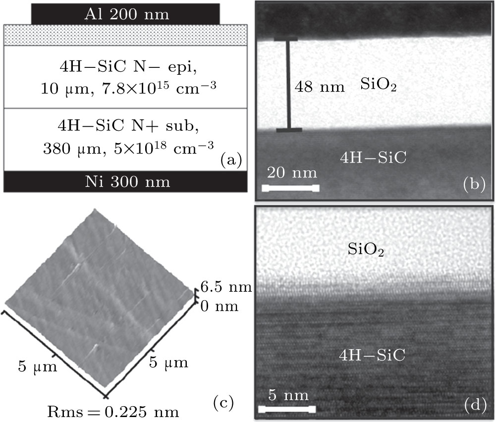
1. IntroductionSilicon carbide (SiC) based metal–oxide–semiconductor-field-effect power transistors (MOSFETs), as high performance power switching devices, have received a great deal of attention, prompted due to a growing need for electric power conversion such as power supplies, motor control, electric hybrid vehicles, traction, and electric power transmission.[1–3] Although SiC power MOSFETs have been commercially available for a few years, the electrical characteristics of SiC power MOSFETs are not understood as well as those predicted from SiC properties.[4]
At the present, the major drawback of the SiC MOSFET is that the poor-quality SiO2/SiC interface and a large number of SiO2/SiC interface states, resulting in large on-resistance, poor oxide reliability and shift in threshold voltage ( under gate-bias stressing.[5–10] For the power conversion area,
  shift under gate bias stressing in SiC MOSFET is as important as the large on-resistance. The instability of threshold voltage is associated with the NIOTs at the SiO2/4H–SiC interface.[4] The NIOT is a kind of oxide trap that is close to the interface and can communicate with the semiconductor substrate.[11] This kind of trap has been described by several different names such as slow trap,[12] border trap,[11] and slow interface state.[13] There is no clarified conclusion about the compositions and structures of NIOTs. Possible explanations, proposed by reported theoretical or experimental results, are that they are carbon clusters, silicon sub-oxide (SiyOx) or silicon interstitials.[14–20] Therefore, it is quite necessary to investigate the relative electrical properties of the NIOTs in SiC MOS capacitors prepared by different post oxidation annealing (POA) processes for better understanding the issue of instability threshold voltage.[21–24]
In this paper, the SiO2/SiC MOS capacitors are fabricated on 4° off-axis 4H–SiC (0001) n-type epitaxial wafers with 1300 °C thermal oxidation, and then annealed at 1175 °C CN2 for 2 h and 1175 °C NO for 2 h, respectively. The SiC MOS capacitors are characterized by means of high frequency hysteresis capacitance–voltage (C–V) characteristics, sequential C–V sweeps, constant voltage stress (CVS) measurements, and gate leakage current performance. The corresponding phenomena are discussed in depth.
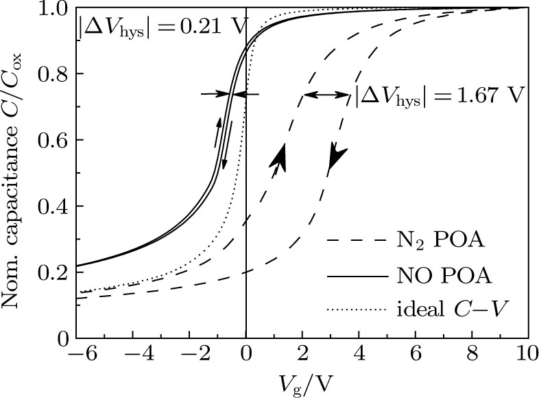
3. Results and discussionFirstly, to extract the total density of the NIOTs, we carry out the initial high frequency (100 kHz) hysteresis C–V characteristic measurements at room temperature for fabricated SiO2/4H–SiC MOS capacitors as shown in Fig. 2. The gate voltage was swept from the deep depletion region (D) to accumulation (A) and then back towards inversion. It can be seen that there is an obvious hysteresis voltage,
where

and

are the flat-band voltage of the forward

and reverse

curves, respectively.
As is well known, the hysteresis can be effectively suppressed by the NO POA process. This hysteresis is due to the generation of NIOTs whose response time is much slower than the interface traps, and is used to characterize the near-interface oxide traps. The density of near-interface oxide traps ( can conveniently be calculated using the flat-band voltage shifts from the following equation:
where
A is the area of the fabricated MOS cap,

is the maximum dielectric capacitance in the accumulation region, and
q is the electron charge. The values of

are calculated to be

and

for N
2 and NO POA samples, respectively. Here, our results are in agreement with the results reported previously
[25–27] that NO POA can obviously reduce the density of NIOTs in SiC MOS.
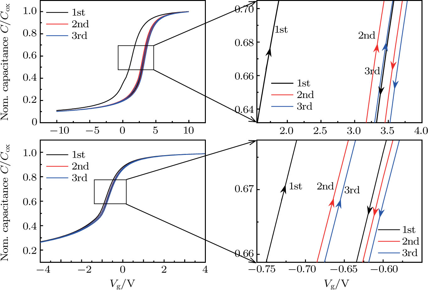
To further study the difference between NIOTs in N2 POA and NO POA samples, we perform the sequential hysteresis C–V sweeping for SiC MOS capacitors. There is no sojourn time in the accumulation region nor in the inversion region in the C–V scanning process. Figure 3 presents the sequential hysteresis C–V characteristics of the N2 POA and NO POA samples, showing a larger hysteresis voltage in the first sweep (that is, the initial curve as shown in Fig. 2), between the forward  and reverse
  curve. However, in the following second and third scanning, the hysteresis voltage is only 0.25 V, much smaller than that in the first sweep. The hysteresis voltages are almost the same in the following two scannings. Both the N2 POA sample and NO POA sample show similar behaviors. We think that the first larger hysteresis is mainly attributed to electrons trapping at NIOTs, including “fast” and “deep” NIOTs, from which the total
  can be obtained.
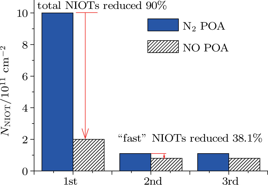
After the initial measurement, a number of electrons are trapped in those “slow” NIOTs with a longer time constant, and those charges cannot be released in the following back scanning (A to D). Therefore, the initial C–V curve cannot be obtained any more during the later measurements. The smaller hysteresis in the following sweeps is attributed to those “fast” NIOTs, which have a short time constant and can exchange electrons with the 4H–SiC during measurements. So the two kinds of NIOTs can be disclosed and extracted by the sequential hysteresis C–V sweeping technique. The different values of  can be extracted from the 1st, 2nd, and 3rd hysteresis C–V for the two samples. The densities of the “fast” NIOTs are determined to be
  and
and  for the N2 POA sample and NO POA sample. The densities of “slow” NIOTs are
  and
and  for the NO POA sample and N2 POA sample, respectively. The comparison between “fast” and “slow” NIOTs in the N2 POA sample and NO POA sample are given in Fig. 4. It is indicated that the “slow” NIOTs can be significantly reduced by the NO POA compared with the N2 POA process, which might be mainly due to an accumulation of N atoms at the interface and an enhanced N passivation effect based on the NO POA. However, here we find that the effect of the NO POA on those “fast” NIOTs is not so effective. In addition, we also can observe that the hysteresis CV curves overall shift toward a more positive direction in the scanning process, but the degrees of those shifts are small, which corresponds with electrons filling in bulk oxide traps (BOTs) during the voltage stress. Although there is no sojourn time in the accumulation region nor in the inversion region in the C–V scanning process, the scanning process can be thought of as a short time bias stressing process. The effect of the constant voltage stress (CVS) on the SiC MOS structure is presented in the following section.
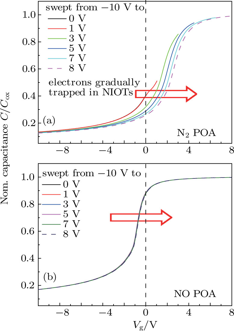
Cycle C–V measurements, whose details can be found in Ref. [24], are performed at room temperature to evaluate the charge trapping characteristics in NIOTs. The gate voltage is first swept from −10 V to 0 V, and then, extended to 1 V, 3 V, 5 V, 7 V, and 8 V. Figure 5 shows the typical results of the cycle C–V measurements for the N2 POA sample and NO POA sample. It shows that the C–V curve shifts toward more positive voltage as the maximum gate voltage increases from 0 V to 8 V. That is due to the electrons trapped into the NIOTs. The degree of the electrons trapped in NIOTs is strongly dependent on the maximum gate voltage, which implies that the main mechanism of the electrons capturing process in NIOTs is probably due to the electrons direct tunneling or the trap assisted tunneling process through the interface state. Compared with the N2 sample, the change of C–V curve shift in the NO sample is very small and can be ignored, indicating the lower density of the NIOTs.
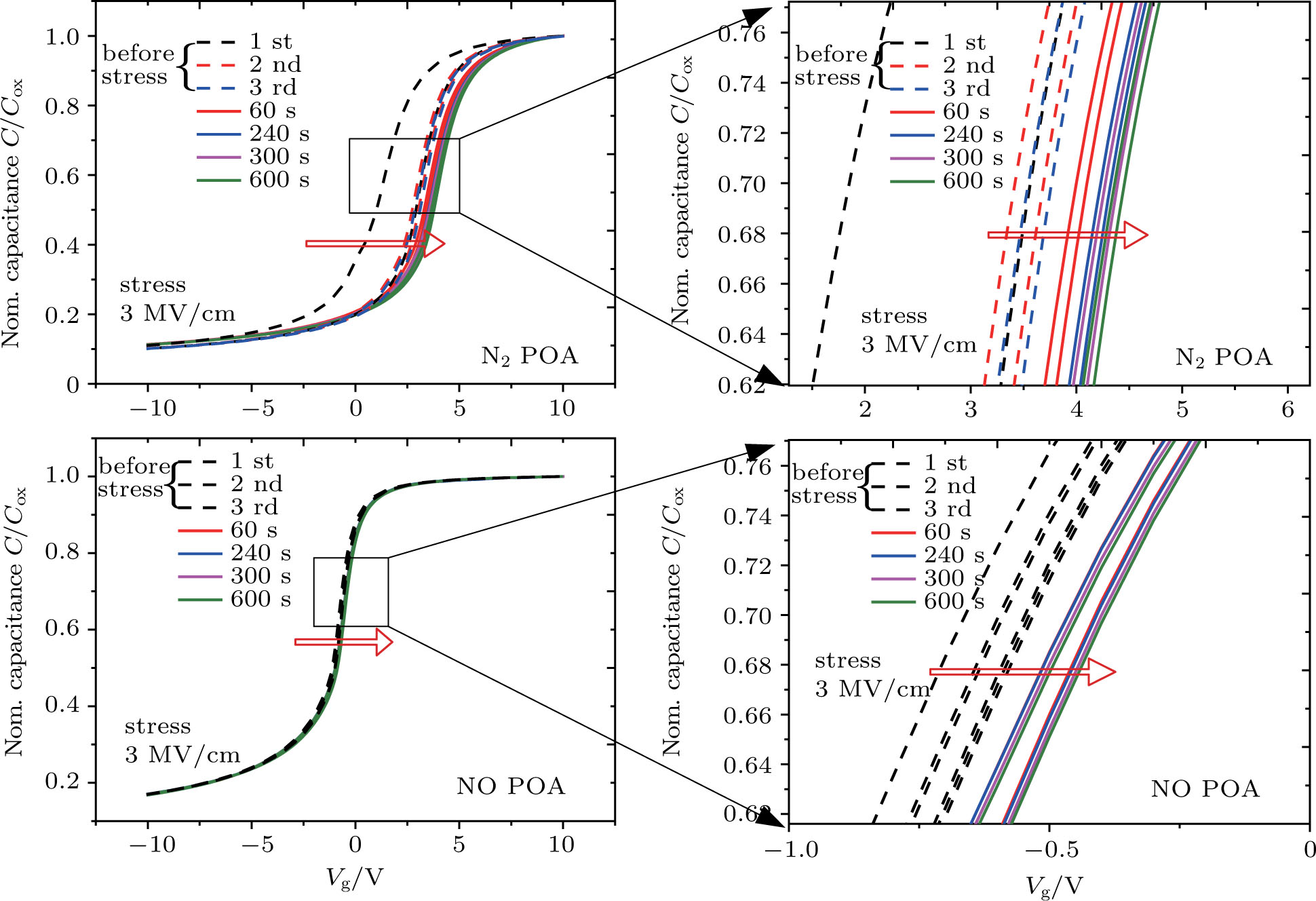
Next, the positive and negative constant voltage stress (CVS) measurements are carried out. Figure 6 shows the hysteresis C–V characteristic loops of the N2 POA sample and NO POA sample with different stress times. The stress gate voltage is fixed at +14 V, corresponding to an electric field of about +3 MV/cm. No matter whether the sample is N2 POA or NO POA, the HF C–V curves all shift toward the more positive direction and are gradually saturated as the stress time increases, indicating negative charge generation in the gate SiO2 layer. This may be due to the electrons trapped in NIOTs and BOTs in the gate oxide layer. It can also be observed that the amplitude of the flan-voltage variation in the NO POA sample is far smaller than that in the N2 POA sample. From the shift of the  in the
  curve from that ideal
  , the effect fixed SiO2 charge (
 ) is obtained from the following equation:
where

is the flat-band voltage of the forward scanning
C–
V curve after the stress,
A is the area of the fabricated MOS cap,

is the maximum dielectric capacitance in the accumulation region, and
q is the electron charge.
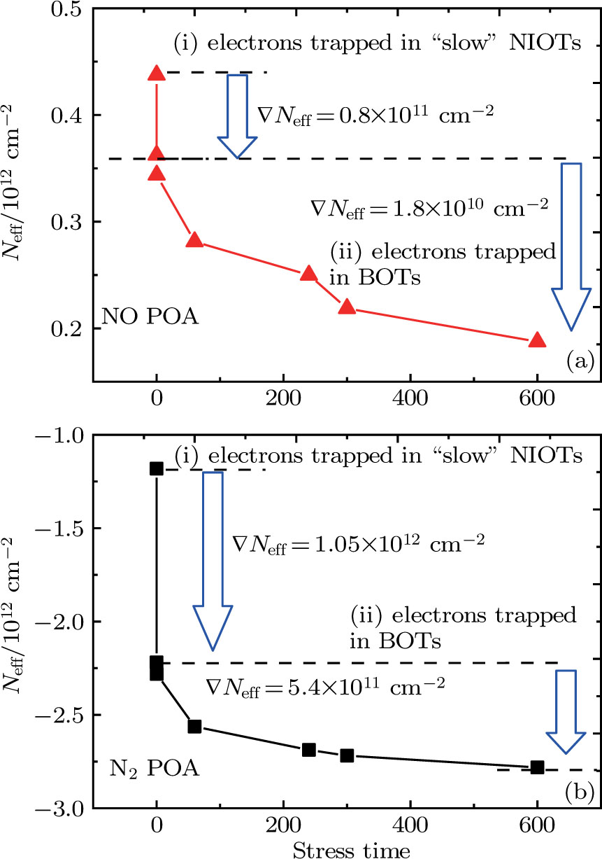
The  as the function of the stress time is present in Fig. 7. The values of
  measured in this way include not only the fixed oxide charge, but also bulk oxide trapped charges, movable charges and the near-interface trapped charges. Overall, these results indicate that
  decreases with the stress time increasing. It is worthwhile pointing out that there is a rapid increase of the
  after the first stress, so this charging process is very short. We think that the increase in
  in this process is attributed to the NIOTs filled with electrons, and the values of
  are determined to be about
  and
and  for NO and N2 POA samples, respectively, which agree well with the results obtained from the aforementioned sequential hysteresis C–V sweeps. Next, the variation of
  becomes slow with the stress time increasing. This process might be caused by the bulk oxide traps filled with electrons. The densities of the bulk oxide traps (
 ) from this stage are determined to be about
  and
and  for the NO POA sample and N2 POA sample, respectively. It should be mentioned that the CVS measurements give the density of filled bulk oxide traps, thus the absence of saturation in Fig. 7 implies that the true total density of bulk oxide traps in the SiO2 film must be higher. After removing the +3 MV/cm CVS, the negative CVS under the −3 VM/cm condition is performed. Very small changes in C–V curves are observed after a certain time of the negative CVS process for both the NO POA sample and N2 POA sample. This reveals that electrons captured by those “slow” NIOTs and BOTs are hardly emitted by the reverse −3 MV/cm voltage stress. From Fig. 7, we can also observe that the sample prepared by NO POA has positive
  , however the
  in the N2 POA sample is negative. Before the CVS measurement, the corresponding values of
  vary from
  to
to  for the N2 POA sample and NO POA sample. This result can be explained as that the interfacial nitrogen species introduced by the NO POA are accumulated at the SiO2/4H–SiC interface, incorporated into carbon clusters (C-clusters) and thus form positively charged interface donors (N+-donors),[28] leading to the variation of the
  .
.
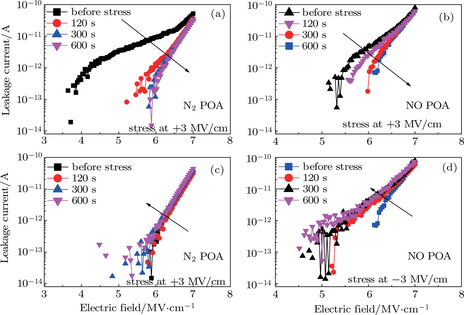
The gate leakage currents as a function of gate voltage under constant voltage stress (+3 MV/cm and −3 MV/cm) with different stress times for NO and N2 POA sample are shown in Fig. 8. In the +3 MV/cm stress process, the gate leakage current always decreases with stress time increasing for both the NO POA sample and N2 POA sample. Especially, in the N2 POA sample it is observed that the initial decreasing amplitude of the gate leakage current reduction is larger than that of the following stress process as shown in Fig. 8(a). This larger decrease of leakage current is attributed to electrons first trapped in “slow” NIOTs. After the initial larger reduction in leakage current, the leakage current decreases very slightly and is saturated soon after stress, which may be due to an electron trapped in bulk SiO2 defects. Those results further confirm that the shift of flat-band voltage initially is caused by the NIOTs communicating with underlying 4H–SiC through tunneling at the beginning of constant voltage stress. Comparing with the N2 POA sample, the degree of the leakage current reduction in the NO POA sample is not so serious as that shown in the N2 POA sample and has a slight variation. It is worthwhile pointing out that the electron generation suggested from the C–V curve shifts conflicts with the electrons trapping suggested from the variation of the leakage current. The effects of the −3 MV/cm stress on the leakage current are presented in Figs. 8(c) and 8(d) for the N2 POA sample and NO POA sample, respectively. It implies that the leakage current increases slightly with the stress time increasing, but the level of the increase is negligibly small, revealing that electrons captured by those NIOTs and BOTs are hardly emitted by the reverse −3 MV/cm voltage stress. It is exactly consistent with the conclusion obtained from the above C–V characteristics.


