


Plasma-assisted surface treatment for low-temperature annealed ohmic contact on AlGaN/GaN heterostructure field-effect transistors
Cite this Article
Wang Lei, Zhang Jiaqi, Li Liuan, Maeda Yutaro, Ao Jin-Ping. Plasma-assisted surface treatment for low-temperature annealed ohmic contact on AlGaN/GaN heterostructure field-effect transistors. Chinese Physics B, 2017, 26(3): 037201 
Permissions
Plasma-assisted surface treatment for low-temperature annealed ohmic contact on AlGaN/GaN heterostructure field-effect transistors
† Corresponding author. E-mail:
Abstract
In this study, a low-temperature annealed ohmic contact process was proposed on AlGaN/GaN heterostructure field effect transistors (HFETs) with the assistance of inductively coupled plasma (ICP) surface treatment. The effect of ICP treatment process on the 2DEG channel as well as the formation mechanism of the low annealing temperature ohmic contact was investigated. An appropriate residual AlGaN thickness and a plasma-induced damage are considered to contribute to the low-temperature annealed ohmic contact. By using a single Al layer to replace the conventional Ti/Al stacks, ohmic contact with a contact resistance of 0.35 Ω·mm was obtained when annealed at 575 °C for 3 min. Good ohmic contact was also obtained by annealing at 500 °C for 20 min.
Keyword:AlGaN/GaN HFET;low-temperature ohmic contact;inductively coupled plasma (ICP);surface treatment
1. Introduction
AlGaN/GaN heterostructure field-effect transistors (HFETs) have advantages to develop high-frequency and high-power devices owing to the high electron mobility, high saturation velocity and high electron density of the two-dimensional electron gas (2DEG) channel.[1–6] To improve the performances of AlGaN/GaN HFETs, a self-aligned-gate (SAG) structure was proposed to decrease the access resistance.[7] In the SAG structure, T-shaped Schottky gate is fabricated firstly as a mask directly for the ohmic metal evaporation. After that, it is necessary to anneal the Schottky gate and the ohmic electrodes simultaneously in order to obtain a good ohmic contact. To avoid degradation of the Schottky contact after annealing at high temperature (commonly above 800 °C for the AlGaN/GaN HFETs), one way is to find a gate material which can withstand the high-temperature annealing.[8] Another way is to reduce the ohmic contact annealing temperature[9] or even develop a non-annealing ohmic process.[10] Furthermore, dielectrics such as 

In our previous work, with the assistance of inductively coupled plasma (ICP) treatment on the surface of ohmic contact area, good ohmic behavior between the metal stack and the semiconductor could be realized at a relatively low annealing temperature of 575 °C and short annealing time of 1 min. It was found that the ohmic contact resistance showed a strong relationship with the ICP treatment conditions.[14] However, the effect of the ICP treatment on the treated surface was not evaluated in detail. The formation mechanism of the low-temperature ohmic contact was not clear, especially on the point of which factor, the lattice damage caused by the ICP treatment or the thinning of the AlGaN layer, takes more important role to the formation of the low-temperature ohmic contact.
Herein, the ICP plasma-assisted low annealing temperature ohmic contact on the AlGaN/GaN heterostructure was investigated to verify the formation mechanism. Samples with entirely-treated surface were fabricated to evaluate the effect of the ICP treatment process on the 2DEG channel. By using a low melting point metal Al to replace the conventional Ti/Al stack, an optimized ohmic contact was achieved with an annealing temperature as low as 500 °C.
2. ICP surface treatment and device fabrication
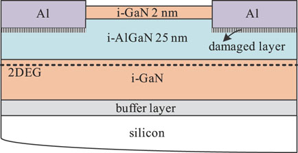
The epitaxial wafers of the AlGaN/GaN HFETs used in this experiment were grown by metal organic chemical vapor deposition (MOCVD) on a high resistance silicon substrate. It consists of a buffer layer, a 1 μm i-GaN, a 25 nm i-AlGaN, and a 2 nm i-GaN from the bottom to the top. The Al mole fraction of the AlGaN layer is approximately 25%.
To evaluate the effect of ICP treatment on the surface and to verify the formation mechanism of low-temperature ohmic process for AlGaN/GaN heterostructure, two groups of samples with the transmission line model (TLM) patterns were prepared by plasma-assisted treatment using an ICP system (Fig. 

 | Fig. 1. (color online) Cross sectional view of the devices fabricated on an entirely-treated surface. |
Samples used to evaluate the ohmic contact at low annealing temperature were also prepared. After sample cleaning, the surface of the samples were treated partially on the ohmic contact area after mesa isolation (Fig. 
 | Fig. 2. (color online) Cross sectional view of the evaluation structure fabricated on a partially-treated surface. |
3. Results and discussion
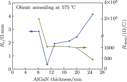
We firstly evaluated the ohmic contact on the entirely-treated (treating power/bias power were fixed at 100/100 W) AlGaN/GaN surface with different residual AlGaN thickness. The surface roughness for all samples after ICP treatment are comparable as confirmed by AFM (approximately 0.6 nm in 5 × 5 μ 

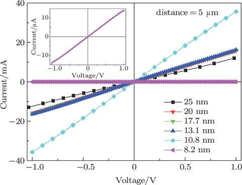 | Fig. 3. (color online) Current–voltage (I–V) characteristics recorded on the TLM patterns with an interval of 5 μm. Inset: residual AlGaN thickness is 8.2 nm. |
The sudden increase of the sheet resistance at the residual AlGaN layer of less than 8.2 nm is possibly due to the weakened piezoelectric effect. By using a transconductance-capacitance method on an FATFET, the electron mobility and electron sheet density of the entirely-treated AlGaN/GaN HFETs were measured and shown in Fig. 


 | Fig. 4. (color online) Ohmic contact resistance (   |
 | Fig. 5. (color online) The dependency of mobility and sheet density on residual AlGaN barrier thickness. Inset is the corresponding transfer characteristics of transistors fabricated on the recessed surface. |
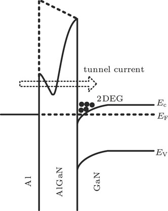
The ICP damage was also reported to introduce n-type doping (N-vacancies),[7] which will upshift the Fermi level at the surface of the AlGaN. Fermi level close to the conduction band edge can decrease the effective Schottky barrier height (SBH) for electron transport (Fig.
 | Fig. 6. Band diagram of the surface-treated AlGaN/GaN heterostructure with Al electrode. |
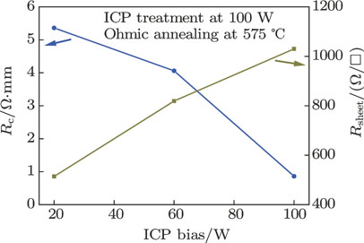 | Fig. 7. (color online) ICP bias dependence of the ohmic contact resistance (   |
It should be mentioned that good ohmic contact could not be obtained using this low-temperature process if the conventional Ti/Al-based metal stack was utilized. Compared with the Al electrode, the TLM result of the Ti/Al/Ti/Au electrode confirms that the existence of Ti would hindrance the contact between Al and the AlGaN, deteriorating the ohmic contact. A possible reason is related to the formation mechanism on AlGaN/GaN heterostructure. The formation of the N vacancy caused by plasma treatment brings merit for the ohmic contact formation, which agrees well with some literatures using the conventional Ti/Al/Ti/Au or Ti/Al/Ni/Au stacks.[16–19] However, the annealing temperatures in their works were still around 800 °C. For the conventional Ti/Al-based metal stack, Ti will react with AlGaN layer under high temperature annealing to generate N vacancy in the AlGaN.[20] N vacancy then create a highly-doped n-type region in the proximity of the interface and decrease the contact resistance between Al and AlGaN. However, in the low-temperature (below 600 °C) annealed ohmic contact process, Ti will nearly not react with AlGaN because of the extremely high melt point (approximately 1678 °C). Therefore, for the plasma-assisted surface treatment, the damage-induced n-type doping layer (N-vacancies) can fill up the function of Ti and Al single layer is much suitable to obtain a low-temperature annealed ohmic contact.
To verify the ohmic contact at a lower annealing temperature of 500 °C, we used samples with ICP-treatment only in the ohmic area for evaluation. The remained AlGaN thickness was approximately 10.8 nm with both ICP and bias power of 100 W. After annealed at 500 °C for 5–30 min (Fig. 

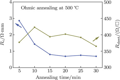 | Fig. 8. (color online) Dependence of the ohmic contact resistance (   |
4. Conclusions
In conclusion, the mechanism of a low-temperature annealed ohmic contact on AlGaN/GaN HFETs with the plasma-assisted surface treatment was verified. Both the N vacancies caused by the ICP damage and the reducing of AlGaN thickness during the ICP treatment are beneficial for obtaining a low-temperature annealed ohmic contact. A low ohmic contact can be achieved by using a single Al layer to replace the conventional Ti/Al stacks. With the assistance of the ICP treatment, an ohmic contact with a contact resistance of 0.35 Ω·mm and a contact resistivity of 1.10 

Reference
| [1] | |
| [2] | |
| [3] | |
| [4] | |
| [5] | |
| [6] | |
| [7] | |
| [8] | |
| [9] | |
| [10] | |
| [11] | |
| [12] | |
| [13] | |
| [14] | |
| [15] | |
| [16] | |
| [17] | |
| [18] | |
| [19] | |
| [20] |