Plasma-assisted surface treatment for low-temperature annealed ohmic contact on AlGaN/GaN heterostructure field-effect transistors
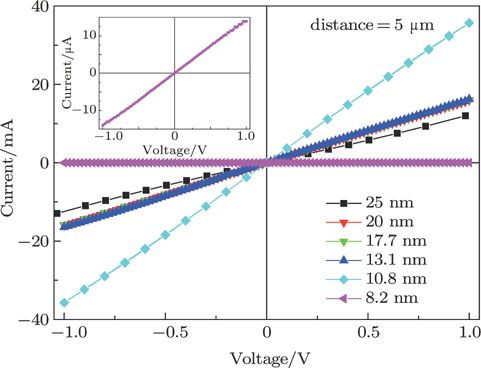
(color online) Current–voltage (I–V) characteristics recorded on the TLM patterns with an interval of 5 μm. Inset: residual AlGaN thickness is 8.2 nm.
