†Corresponding author. E-mail: xrluo@uestc.edu.cn
*Project supported by the National Natural Science Foundation of China (Grant Nos. 61176069 and 61376079) and the Program for New Century Excellent Talents at the University of Ministry of Education of China (Grant No. NCET-11-0062).
An ultra-low specific on-resistance ( Ron,sp) oxide trench-type silicon-on-insulator (SOI) lateral double-diffusion metal–oxide semiconductor (LDMOS) with an enhanced breakdown voltage ( BV) is proposed and investigated by simulation. There are two key features in the proposed device: one is a U-shaped gate around the oxide trench, which extends from source to drain (UG LDMOS); the other is an N pillar and P pillar located in the trench sidewall. In the on-state, electrons accumulate along the U-shaped gate, providing a continuous low resistance current path from source to drain. The Ron,sp is thus greatly reduced and almost independent of the drift region doping concentration. In the off-state, the N and P pillars not only enhance the electric field ( E-field) strength of the trench oxide, but also improve the E-field distribution in the drift region, leading to a significant improvement in the BV. The BV of 662 V and Ron,sp of 12.4 mΩ·cm2 are achieved for the proposed UG LDMOS. The BV is increased by 88.6% and the Ron,sp is reduced by 96.4%, compared with those of the conventional trench LDMOS (CT LDMOS), realizing the state-of-the-art trade-off between BV and Ron,sp.
In order to increase the breakdown voltage (BV) for a conventional high voltage lateral double-diffusion metal– oxide semiconductor (LDMOS), it is necessary to reduce the drift region doping concentration (Nd) and increase the drift region length (Ld). For a high voltage LDMOS, the specific on-resistance (Ron, sp) is mostly determined by the Nd and Ld, resulting in the silicon (Si) limit of Ron, sp ∝ BV2.5.[1– 3] The reduced surface field (RESURF) technology (including single/double/triple RESURF) is widely used to improve the trade-off between the Ron, sp and BV. However, it is useless for reducing the cell pitch and thus restricts further reduction of the Ron, sp.[4– 6, 7] A dielectric trench inserted in the drift region for LDMOS not only improves the BV, but also dramatically reduces the Ron, sp by shortening the device cell pitch.[8– 11] However, a conventional deep trench is not suitable for high voltage application (e.g. BV > 600 V) because of its weakened RESURF effect and a corresponding low Nd. Therefore, the enhanced bulk field (ENBULF) concept is proposed to improve the BV and reduce the Ron, sp.[12] Unfortunately, the Nd is still the key limit of the Ron, sp for existing MOSFETs with RESURF and trench technologies. The extended gate is used to enhance the conductance in the drift region in the on-state without compromise in the off-state BV.[13] However, it has an intrinsic high leakage current from gate to drain under the high gate– source voltage. Moreover, as a planar LDMOS, it is also helpless for reducing the cell pitch, which restricts the decrease of the Ron, sp.
In this paper, an SOI trench LDMOS with a U-shaped gate is proposed to realize a significant trade-off between Ron, sp and BV. The current transports through the electron accumulation layer from source to drain. Consequently, the Ron, sp greatly decreases and exhibits less dependence on the Nd. This current transport mode is different from that of the existing MOSFETs. In the off-state, the depleted N/P pillars enhance the E-field strength of the trench oxide and the drift region, leading to a higher BV. Thus, an ultra-low Ron, sp and high BV are obtained.
Figure 1(a) shows the schematic cross-section view of a UG LDMOS. An oxide trench is built into the drift region, and a U-shaped gate surrounding the trench extends from source to drain. In the U-shaped gate semiconductor, the P-pillar is adjacent to the P+ region under the gate electrode, extending to the bottom of the trench. One side of the N-pillar touches the P-pillar at the trench bottom, and the other side contacts the PN junction (DR) connected to the drain electrode (D). The DR is reversely biased to sustain the gate– drain voltage (VGD) in the on-state. In Fig. 1(a), Tsi, Tox, Tt, and Tdox are the thickness values of the active region, the buried oxide (BOX) layer, the trench, and the gate oxide layer, respectively. Wt and W are the widths of the trench and the device respectively.
 | Fig. 1. (a) Schematic cross-sectional view of the UG LDMOS. (b) Working mechanism of the gate structure in on-state. (c) Charges distribution in the off-state. |
Figure 1(b) shows the operation mechanism of the gate structure (marked with the dashed rectangle in Fig. 1(a)) in the on-state. It indicates the electron distribution and the equivalent resistances of the drift region. Meanwhile, the equivalent metal– insulator– semiconductor (MIS) capacitance between the U-shaped gate structure and the drift region is also demonstrated. When VGS > VDS, electrons accumulate along the sidewall of the U-shaped gate oxide caused by the MIS structure mentioned above. Further, electrons flow through the inversion channel and the accumulation layer at VGS > Vth (Vth: threshold voltage), forming a continuous ultra-low resistance path. The VGD is sustained by the reversely biased DR in Fig. 1(a).
The on-resistance of the drift region (R) consists of two resistances connected in parallel in Fig. 1(b): the accumulation layer resistance (RC) and the resistance RD determined by the doping concentration. In general, RC ≪ RD and thus R ≈ RC. Additionally, the P-pillar has an assisted depletion effect on the N-drift region in the off-state, allowing a higher Nd and a lower RD. Therefore, the total drift region resistance is significantly reduced.
Figure 1(c) shows the charge distribution in the off-state for the UG LDMOS. The off-state operation mechanism is given as follows.
First, the lateral BV (BVlat) is sustained mainly by the oxide trench. It can be given by

where Etx is the horizontal E-field strength in the oxide trench. The fully depleted N/P pillars beside the oxide trench provide an additional E-field Δ Etx as shown in Fig. 1(c). As a result, the Etx and the BVlat are enhanced.
Second, the vertical BV (BVver) is sustained by the Si layer (VSD) and the BOX layer (VI) under the drain. These can be written as
 |
 |
 |
where EI and ES are the E-field strengths of the BOX and the Si at the Si/BOX interface respectively; ε S and ε I are their relative permittivities of Si and BOX; σ in is the charge density at the BOX interface. Note that holes and electrons are induced at the interface of the BOX, as illustrated in Fig. 1(c). VI and BVver are improved.
Third, the voltage sustained by the BOX layer is equal to that sustained by the Si layer under the source (VSS). Because both the source and substrate are grounded, equation (2) can also be expressed by

The electric characteristics are investigated with simulator MEDICI. The device structure parameters used in the simulation are given as follows: W = 15.0 μ m, Wt = 9.0 μ m, Tsi = 25.0 μ m, Tox = 1.0 μ m, Tt = 21.0 μ m, and Tdox = 0.1 μ m.
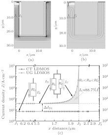
Figures 2(a) and 2(b) show the two-dimensional (2D) flow line distributions of the UG LDMOS and CT LDMOS in the on-state, respectively. In the UG LDMOS, a high-density electron accumulation layer is induced beside the U-shaped gate. As a result, the current density through the accumulation layer is very high and the current herein achieves 88.7% of the whole current (by integral verification) in Fig. 2(c). Additionally, owing to the charge compensation between the N-drift region and the P-pillar, the optimal Nd of 2.2 × 1015 cm− 3 is higher for the UG LDMOS. However, the Nd of 3.4 × 1014 cm− 3 is very low in the CT LDMOS because the RESURF effect is weakened by a deep trench. The current determined by the Nd is improved (Δ ID1), (although the cross section of the current in CT LDMOS is slightly wider than that in UG LDMOS, i.e. 
Figure 3 shows the equi-potential contours at breakdown. The voltage drop along the trench surface (i.e., the D → A direction) is equal to that around the trench (i.e., along the D → C → B → A direction), which represents that the oxide trench folds the drift region and thus increases the effective drift region length. In the UG LDMOS, as the N/P pillars enhance the E-field strength in the oxide trench (along D → A) and optimize the E-field strength around the trench (along D → C → B → A), the equi-potential contours in the trench region and the drift region are uniform compared with those of the CT LDMOS. The double-headed arrows in Fig. 3 indicate the voltage drops in Si under the source and drain. Owing to the N/P pillars, VSS increases from 233 V to 340 V and VSD from 118 V to 322 V. According to Eq. (3), the BV of the UG LDMOS increases to 662 V compared with the 351 V of the CT LDMOS at the same cell pitch of 15 μ m.
 | Fig. 3. Equi-potential contours at breakdown voltage for (a) UG LDMOS (662 V) and (b) CT LDMOS (351 V). |
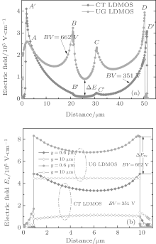
Figure 4(a) provides the E-field distributions around the trench. The N/P pillars in the UG LDMOS introduce two new E-field peaks at the bottom of the trench (points B and C), which improve the E-field in the drift region. However, the E-field strength is low near the trench bottom (e.g., points B′ and C′ ) for the CT LDMOS. Figure 4(b) shows the horizontal E-field (Etx) distributions at the surface and bulk of the oxide trench. The surface field of UG LDMOS increases to 8.3 × 10⁵ V/cm from 4.9 × 10⁵ V/cm of the CT LDMOS, with an additional E-field Δ Etx ≈ 3.4 × 10⁵ V/cm. Meanwhile, in the bulk (y = 10 μ m), the E-field strength increases by about 3.4 × 10⁵ V/cm. Therefore, the BVlat is considerably improved as indicated in Eq. (1).
The E-field and potential distributions under the drain and source are shown in Fig. 5(a). The N/P pillars improve the E-field distribution of the UG LDMOS, leading to higher voltages sustained by the drift regions under source (VSS) and drain (VSD). The BVver is thus considerably improved as shown in Eq. (3). Figure 5(a) also illustrates Eq. (2) and VI = VSS. Meanwhile, the top interface potential of the BOX layer is clamped, and thus the potential drop across the BOX remains a constant of VI = VSS = 340 V. As a result, lots of holes and electrons are adaptively induced at the top and bottom interfaces of the BOX. The potential distributions along the top surface of the BOX layer are independent of the Tox before the dielectric breakdown. Figure 5(b) illustrates the E-field strengths of the BOX layer at breakdown with the different Tox values. More than 5 × 1018 cm− 3 holes and electrons accumulate at the opposite interfaces of the BOX layer. The charge density is adaptive to maintain the constant VI value at the different Tox values. According to Eq. (2) mentioned above, the E-field distributions of the BOX layer (EI) are enhanced adaptively with different values of Tox. The E-field of the BOX layer increases from 170 V/ μ m to 678 V/ μ m with Tox decreasing from 2.0 μ m to 0.5 μ m.
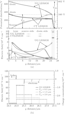 | Fig. 5. (a) Electric field and potential distributions under drain and source. (b) Electric fields of the BOX layer at breakdown with different values of Tox (x = 14.0 μ m). |
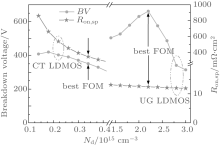
Figure 6 reveals the influences of Nd on BV and Ron, sp. For the CT LDMOS, the Ron, sp increases by 206.8% (from 280.5 mΩ · cm2 to 860.5 mΩ · cm2) when Nd decreases by 66.7% (from 4.2× 1014 cm− 3 to 1.4× 1014 cm− 3). However, the Ron, sp of the UG LDMOS increases only by 9.2% (from 11.9 mΩ · cm2 to 13.1 mΩ · cm2) when Nd decreases by 53.3% (from 3.0× 1015 cm− 3 to 1.4× 1015 cm− 3). Therefore, for the UG LDMOS, the Ron, sp is not only extremely low but also almost independent of the Nd. It means that the highest figure of merit (FOM) (FOM = BV2/Ron, sp) is obtained at the highest BV for the UG LDMOS. Consequently, the Nd is chosen to obtain the highest BV without influence on the Ron, sp for the UG LDMOS. However, the optimal Nd of the CT LDMOS is chosen by taking the trade-off between the Ron, sp and the BV into account. This is an important advantage of the UG LDMOS over the CT LDMOS. Moreover, the BV of the UG LDMOS is superior to that of the CT LDMOS.
Table 1 summarizes the optimized characteristics of Nd, BV, Ron, sp, and FOM for the UG LDMOS, CT LDMOS, ENBULF LDMOS (Ref. [12]), and the latest TLDMOS (Ref. [11]). It reveals that simple trench technology cannot achieve optimal trade-off between the BV and the Ron, sp in the case of high voltage application because of the weakened RESURF effect.
| Table 1. Optimized characteristics for the UG LDMOS, CT LDMOS, ENBULF LDMOS, and TLDMOS. |
Figure 7 shows a comparison of the Ron, sp versus BV among the UG LDMOS, different RESURF LDMOSFETs (including single/double/triple RESURF) in Ref. [7], ENBULF LDMOS and the latest TLDMOS. Apparently, the Ron, sp of the UG LDMOS is far lower than those of the others. The UG LDMOS obtains a state-of-the-art trade-off between Ron, sp and BV at different voltage levels.
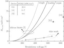 | Fig. 7. A comparison of Ron, sp versus BV for UG LDMOS among different RESURF effects, ENBULF LDMOS, and the latest TLDMOS. |
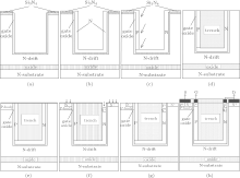
Figure 8 shows the feasible key process steps to fabricate a prototype UG LDMOS: (a) etch the SOI material (with an oxide layer and an Si3N4 shielding layer) and then thermally grow to form the gate oxide layer; (b) deposit a certain doped N-type polysilicon, chemical– mechanical planarization (CMP) and etch the polysilicon to form the N-pillar; (c) angled ion implant to form the P-pillar; (d) fill the trench with SiO2 followed by CMP, and then remove the Si3N4 layer and the oxide layer; (e) implant to form the P-body and then thermally grow an oxide layer; (f) etch the N-pillar and implant to form the N+ region of the DR, N+ source /drain region; (g) deposit the P-type region on N+ to form DR followed by CMP; (h) implant to form the body contact region, the gate contact region, and deposit to form the electrodes.
An ultra-low specific on-resistance LDMOS with a U-shaped gate is proposed and investigated by simulation. With the U-shaped gate around the oxide trench, the proposed structure can introduce a high-density electron accumulation layer and provide a low-resistance current path in the on-state. The Ron, sp is sharply reduced and less dependent on the doping concentration of the drift region. With the N/P pillars at the sidewalls of the oxide trench, not only can the UG LDMOS increase the BV but also reduce the Ron, sp. As a result, BV = 662 V and Ron, sp = 12.4 mΩ · cm2 are obtained at a cell pitch of 15 μ m. The proposed UG LDMOS realizes the state-of-the-art trade-off between BV and Ron, sp, compared with the conventional oxide trench LDMOS, RESURF LDMOS, ENBULF LDMOS, and the latest TLDMOS.
| 1 |
|
| 2 |
|
| 3 |
|
| 4 |
|
| 5 |
|
| 6 |
|
| 7 |
|
| 8 |
|
| 9 |
|
| 10 |
|
| 11 |
|
| 12 |
|
| 13 |
|


