An ultra-low specific on-resistance trench LDMOS with a U-shaped gate and accumulation layer

An ultra-low specific on-resistance trench LDMOS with a U-shaped gate and accumulation layer |
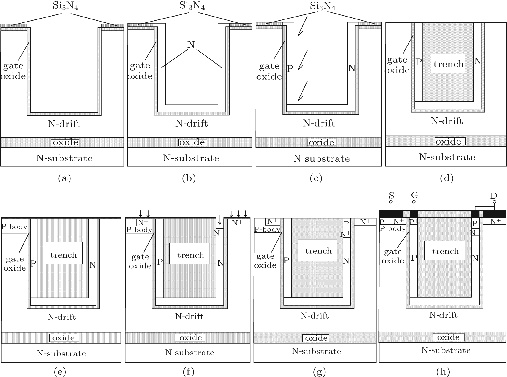
| Key steps of the UG LDMOS: (a) etch trench and form the gate oxide layer, (b) form the N-pillar, (c) form the P-pillar, (d) form the trench, (e) form the P-body, (f) form the N+ region of the D R, N+ source, and drain region, (g) form the P-type region of the D R, (h) form the body contact region, the gate contact region, and electrodes. |
 |