†Corresponding author. E-mail: zhangym@xidian.edu.cn
*Project supported by the Key Specific Projects of Ministry of Education of China (Grant No. 625010101), the National Natural Science Foundation of China (Grant No. 61234006), the Natural Science Foundation of ShaanXi Province, China (Grant No. 2013JQ8012), the Doctoral Fund of Ministry of Education of China (Grant No. 20130203120017), and the Specific Project of the Core Devices, China (Grant No. 2013ZX0100100-004).
This paper reports the performances of Ti/Al based ohmic contacts fabricated on highly doped p-type 4H-SiC epitaxial layer which has a severe step-bunching surface. Different contact schemes are investigated based on the Al:Ti composition with no more than 50 at.% Al. The specific contact resistance (SCR) is obtained to be as low as 2.6 × 10⁻⁶ Ω·cm2 for the bilayered Ti(100 nm)/Al(100 nm) contact treated with 3 min rapid thermal annealing (RTA) at 1000 °C. The microstructure analyses examined by physical and chemical characterization techniques reveal an alloy-assisted ohmic contact formation mechanism, i.e., a high degree of alloying plays a decisive role in forming the interfacial ternary Ti3SiC2 dominating the ohmic behavior of the Ti/Al based contact. Furthermore, a globally covered Ti3SiC2 layer with (0001)-oriented texture can be formed, regardless of the surface step bunching as well as its structural evolution during the metallization annealing.
Silicon carbide (SiC) is more attractively used in a power electronic circuit mainly due to its advantageous properties over silicon (Si) for high-power and high-temperature devices, such as wide bandgap, high critical electric field strength, and high thermal conductivity.[1– 3] With the improvement in the bulk material quality, 4H-SiC unipolar devices for 600 to 1700 V applications are commercially available.[4, 5] However, some technological problems need to be further solved. One of them is the formation of a low-resistance ohmic contact to p-type 4H-SiC, which is specially essential for developing high-performance SiC bipolar devices in order to lower conduction losses and promote the capability of handling surge currents in the order of several thousand amps.
Many studies have been carried out to overcome the intrinsic difficulty in forming such a contact to p-type 4H-SiC, i.e., the large Schottky barrier at the interface due to the work functions of most metals being less than the energy difference between the valence band edge of p-type 4H-SiC and the vacuum level (∼ 7 eV), so as to achieve the best possible results, in terms of the specific contact resistance (SCR). Of all the different solutions, to date, the Ti/Al based metallizations deposited on a heavily doped (> 1019 cm− 3) epitaxial p-type layer have produced the lowest and reproducible SCR value as low as 10− 6 Ω · cm2 when annealed at high temperature up to 1000 ° C, [6] mainly due to the formation of the interfacial ternary Ti3SiC2 with metallic nature and a narrow band gap of 0.12 eV.[7] It has been reported, by combining experimental studies with theoretical investigations, that the heteroepitaxially SiC/Ti3SiC2 interface is responsible for the lowering of the Schottky barrier, based on three main possible models: i) Ti3SiC2 behaves as an intermediate layer to divide the large barrier height into smaller ones, leading to enhanced thermionic emission; [8] ii) interfacial reaction induced point defect states in the near-interface SiC cause Fermi-level pinning or act as trapping centers to assist carrier tunneling and hopping, thus all reducing the effective barrier height; [9] and iii) an atomic C layer trapped at the SiC/Ti3SiC2 interface, together with the formed ordered interfacial terrace, cause gap states at EF in the SiC layer and localized charge accumulation in a spatially connected manner, offering carrier conduction channels to allow current transport across SiC.[10, 11]
To obtain such a low contact resistance from the processing point of view, two structural conditions, combined with the high annealing temperature, seem indispensable for the Ti/Al based contacts. One is a high Al content in the initial metal deposition (generally more than 75 at.% in concentration), which can be helpful for creating a liquid alloy to promote the interfacial reaction.[9– 12] Especially for the Ni/Ti/Al system, a more attractive ohmic contact scheme yielding a stable SCR ranging in the mid 10− 5 Ω · cm2 after relatively low temperature annealing (∼ 800 ° C), [13] a similar contact composition with a high Al amount is still required even though Ni indeed plays an important role in forming the ohmic contact because of its ability to form Ni2Si silicide.[14] In such a rich-Al context, however, a rough contact morphology usually appears in the Ti/Al contact subjected to “ standard” annealing process (e.g., rapid thermal annealing (RTA) above 900 ° C), since an excess of Al spreads out and agglomerates via annealing because of the low melting temperature of Al (660 ° C). This drawback, to some extent, causes a poor lithographic definition of critical metal geometries in the device fabrication.[15] Although Ni/Ti/Al based contacts annealed at a lowered annealing temperature could solve this morphological problem, the achieved SCR values on an epitaxial p+ -type layer are not low enough for higher current capabilities in power electronics applications.[16, 17]
The other crucial condition for approaching state-of-the-art SCR is a pronounced “ smooth” surface morphology of SiC. This was demonstrated by the study on surface morphology dependence of the ohmic behavior of Ti/Al contacts to implanted p-type SiC, [18] where a specific rough surface (i.e., step-bunching) formed as a result of the post-implantation annealing at 1700 ° C without a protective carbon capping layer, gives rise to the formation of a disordered interfacial layer containing discrete Ti3SiC2 grains during metallization annealing, which is at least partially responsible for the degradation in ohmic properties. By contrast, the annealed contacts formed on the epitaxial SiC with a quite flat surface (typical mean surface roughness (RMS) less than 1 nm) exhibit continuous coverage of the textured ternary phase on the SiC surface, together with an epitaxial and atomically abrupt Ti3SiC2/SiC heterointerface.[9, 11] This ordered interface structure facilitating the current flow has been considered as the critical origin of the ohmic nature in the p-type SiC/Ti/Al contact system. Even in the case of non-rich-Al-contained contact, as mentioned by Jennings et al., [6] a perfect ohmic behavior can be experimentally realized based on a hexagonal pattern confirming deposition of Ti film on the p-type SiC epilayer with near-planar surface, thereby forming a matched crystal direction relationship of Ti(0001)//4H-SiC(0001), enhancing the generation of a high degree of orientated Ti3SiC2 at the interface.
However, the surface morphology of epitaxial SiC is expected to be highly sensitive to small variation of the chemical-vapor-deposition (CVD)-grown conditions such as the C/Si ratio, growth temperature, etc., [19] and also to the pre-treatment of the substrate material before an epi-procedure.[20] With regard to the standard Si-C-H based step-mode growth on 4° off-axis 4H-SiC substrate, which is widely employed for the fabrication of SiC based power devices, the as-grown surface usually suffers step-bunching, [21, 22] which is characterized by the similar roughening of the surface with terraces arrangement parallel to the original miscutting angle but different formation mechanism compared with the implanted case. This detrimental effect cannot be completely removed for the hexagonal polytypes with misorientation cut toward the [11 − 20] direction, [23] it even becomes more remarkable with increasing thickness of the epilayers due to an accumulation of the difference in the growth rate between the different basal planes of the stacking sequence[24] or an enhanced nucleation and precipitation of gaseous Si to form Si droplets under the non-optimized growth conditions like a low C/Si ratio.[25] Therefore, it seems necessary to develop a good ohmic contact with both low SCR and flat annealing morphology on the p-type epilayers with a notably bunched surface. However, this particular aspect related to the specific case of Ti/Al ohmic contacts has not been fully addressed so far.
This paper presents a study of low-Al-contained Ti/Al based ohmic contact realized on p+ -type 4H-SiC epilayer with a severe step-bunching surface, principally taking into account the fact that reducing the thickness of the Al layer would be able to improve the surface morphology. The electrical properties of the contacts are investigated upon simple variation of stacking species and annealing conditions. In order to probe the responsible mechanism, this non-ideal ohmic contact system is characterized by combining the optical microscope, x-ray diffraction (XRD), and scanning electron microscope (SEM), and the annealed surface morphology and interfacial microstructure are compared and discussed.
A 3-inch highly doped N+ 4H-SiC substrate (from Cree, Inc.) with 4° -off Si-terminated (0001) surfaces inclined toward the [11 − 20] direction was chosen as a starting material. The homoepitaxial growth was done in a horizontal hot-wall CVD reactor, in which the precursors for the standard process were silane (SiH4) and propane (C3H8) diluted in hydrogen (H2) carrier gas. Prior to growth, the in situ etching process in the pure H2 ambient was carried out at 1580 ° C for 10 min to remove the surface damage or stress of the CMP-treated substrate.[26] The pressure during H2 etching was 100 mbar. The main growth parameters are summarized in Table 1, where the C/Si and Si/H2 ratio were fixed at 1.0% and 0.03%, respectively. The p-type dopant element Al was introduced from trimethylaluminum (TMA). A continuously grown PN-type structure composed of a targeted 0.5-μ m-thick p+ surface layer with a concentration of 1 × 1020 cm− 3 and an unintentionally doped n− layer on a nitrogen-doped n+ buffer layer were finally obtained for the subsequent ohmic contact studies. The thickness and concentration of the p+ layer were measured using secondary ion mass spectrometry (SIMS). The as-grown surface of the epilayer was monitored by Nomarski differential interference contrast optics (NDIC) and in more detail using tapping mode atomic force microscopy (AFM).
| Table 1. Mainly epitaxial growth parameters. |
The prepared epiwafer was cut into 1 × 1 cm2 square dies as required. All samples were then subjected to organic solvents and sulfuric acid/hydrogen peroxide (seven-up) solution cleaning. Four sets of rectangle transmission line method (TLM) mesa structures for each die were determined by inductively coupled plasma (ICP) etching with a sputtered nickel etch mask. After removing the residual masking materials, the SiC surfaces were processed by a standard Radio Corporation of America (RCA) procedure followed by a two-step thermal oxidation process, i.e., 1-h wet sacrificial oxidation at 1100 ° C and a subsequent 3-h dry passivated oxidation at 1150 ° C, which could help to protect and prevent the surface from being contaminated, [27] and probably to create carbon clusters at the interface that facilitates the beginning of the reactions between the metal atoms and the SiC.[28] This thin SiO2 layer with an approximate thickness of 20 nm was patterned via lithography and then etched in buffered oxide etch (BOE) 7:1 solution. Next, metallic stacks were sputtered onto the exposed areas and defined using lift-off in acetone and an ultrasonic bathing system. Table 2 lists the investigated Ti/Al based contact schemes, merely with respect to a low Al content with equal to or less than 50 at.% in concentration. The resulting metallic stacks were annealed using a rapid thermal annealing furnace within an Ar ambient.
| Table 2. Summary of layer contacts (Ti is the first layer deposited on the surface of 4H-SiC). |
The electrical characterization of the contacts was measured with a Cascade probe station using an Agilent B1505A parameter analyzer, and the SCR was calculated according to the TLM arrangement, with seven 550 μ m (W) × 215 μ m (L) rectangle pads separated by 20, 30, 40, 50, 60, and 70 μ m (d), respectively. The annealed contact morphology was examined by optical microscope. XRD with Cu Kα radiation operating at 40 kV and 40 mA was used to identify the compounds formed during thermal annealing. The angle of grazing incidence scanning was fixed at 6° . Further microstructural analysis was carried out by using SEM equipped with chemical etching.
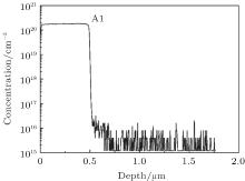
Figure 1 shows the measured SIMS doping profile of the p+ epilayer, from which a nearly constant Al concentration of 1.8 × 1020 cm− 3 in the most p+ region but slightly falling down to 6.7 × 1019 cm− 3 at the outermost surface is observed. The thickness of the growth tail is estimated at less than 10 nm, prospectively as a result of the non-terminated reaction of the residual gases in the chamber during the initial stage of the temperature ramp-down. The surface morphology of the as-grown epilayer is characterized by the NDIC image and AFM scan taken over 5 × 5 μ m2, respectively, as shown in Fig. 2. Obviously, a rough surface with step-bunching but free of other morphological defects can be seen on a macroscopic scale (Fig. 2(a)), in accordance with previous experimental reports on epitaxial growth on 4° off-axis substrates, [22, 29] where removing the step-bunching is found to be contrary to reducing the various types of morphological defects, such as extended triangles. Local feature of the surface (Fig. 2(b)) randomly selected within the central 90% of the wafer area further reveals the level of the surface step-bunching with the RMS value of 5.9 nm and a maximum step height (Δ Z) of 17.1 nm. The huge undulating steps are related to the formation of nonstoichiometric portions of the crystal lattice, composed of metastable Si species such as Si2C and SiC2.[25] This quite rough surface indicates that the current growth conditions are far from optimization even though the in suit H2 etching was also previously reported to be beneficial to reducing the step-bunching effect for growth on the 4° off-axis 4H-SiC substrates.[19] It must be pointed out, additionally, that the thermal oxidation procedures during contact fabrication have little influence on the step-bunching (not shown here), suggestive of an extremely thermodynamic stability of the undesirable surface microstructure.
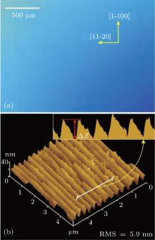 | Fig. 2. Surface morphology characterization of the as-grown epilayer: (a) NDIC image and (b) AFM scan. |
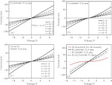
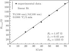
Figures 3(a)– 3(c) display the room temperature I– V measurements as a function of space between pads of the typical TLM patterns for the three contact schemes shown in Table 2, respectively. The first curve (pad 1– 2) for each annealed contact and their similar as-deposited one are also shown in Fig. 3(d) for comparison. All contacts exhibit standard Schottky character before annealing, implying that the highly doping level of the p+ surface layer, which is conducive to the tunnel effect, is not the key point to make the contact characteristics turn into ohmic. The I– V characteristics of the Ti(100 nm)/Al (100 nm) contact system change from nonlinear behavior (or partial Schottky behavior) when annealed at 900 ° C for 5 min (Fig. 3(b)) to linear behavior via annealing at 1000 ° C for 3 min (Fig. 3(a)), suggesting that the annealing temperature plays a more important role in forming the ohmic contact. The SCR value for the ohmic behavior extracted from the RTotal(d) characteristics as shown in Fig. 4, is 2.6 × 10− 6 Ω · cm2, which is very close to the level of state-of-the-art SCR on p-type SiC ever reported in the literature, [6, 30] and more importantly is the lowest SCR value ever obtained on such a severe step-bunching surface to the best of our knowledge. This result is promising for realizing the power devices requiring a lower contact resistance on p-type 4H-SiC. For the triplelayered Ti(100 nm)/Al(100 nm)/Ti(50 nm) contact system, I– V characteristics are not linear after the same annealing as the Ti(100 nm)/Al(100 nm) contact system, i.e., it is still nonohmic for such a sandwich structure (Fig. 3(c)).
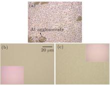
The alloyed contact surface morphologies of the samples are examined by the optical microscope, to preliminarily explain the different electrical behaviors. Figure 5 shows the × 100 photomicrographs of the annealed contact surfaces, together with the as-deposited surfaces for both bilayer and triplelayer contacts (insets of Figs. 5(b) and 5(c), respectively). For the Ti(100 nm)/Al(100 nm) bilayer, it is clear that intense alloying between metals occurs during 1000 ° C annealing (Fig. 5(a)), suggestive of a sufficient liquid alloy existing in the contact layer. Generally, the liquid phase has a high reactivity to the solid (substrate) due to a high diffusitivity for both the solutes and solvents in liquid, thus the chemical reaction of Ti/Al and SiC to form conducting carbide or silicide in a contact/SiC near-interface region easily takes place at an elevated temperature. In addition, a homogeneous contact surface covered with a few Al agglomerates can be obtained due to a low Al content in the contact.
In contrast, annealing at 900 ° C seems invalid in terms of changing the metallic morphology (Fig. 5(b)), indicating that there is no significant liquid trace within the contact when the annealing temperature is lowered even though the annealing time is increased. Looking into the morphology of the annealed contacts and their respective electrical characteristics, it is believed that the presence of high-temperature induced alloying is necessary for the Ti/Al-based contact to obtain an ohmic behavior. However, for the Ti(100 nm)/Al(100 nm)/Ti(50 nm) triplelayer, the slight roughening of the contact surface (Fig. 5(c)) instead of a visible alloyed structure is observed for annealing at 1000 ° C. It is proposed that this is due to the enhanced suppression of the Al-based liquid by an addition of top Ti layer, which has a high melting point (1668 ° C) and is not melted during annealing, blocking melted Al from spreading out and subsequently agglomerating during the cooling stage. From the technological point of view, undoubtedly, the higher annealing temperature is expected to realize alloying for this type of high-Ti-contained contact.
To corroborate the alloying evolution observed from the optical microscope and to further determine the reaction products formed after annealing, the microstructure of the annealed contacts with changed surface morphology, i.e., bilayer and triplelayer after annealing at 1000° C for 3 min, is comparatively evaluated by XRD θ – 2θ scan as shown in Fig. 6, in which the metallic phases are identified using the X’ pert High Score Plus and the 2013 ICDD powder diffraction database. It is evident that the alloyed Ti(100 nm)/Al(100 nm) bilayer shows a prominent Ti3SiC2 phase with strongly (0001)-oriented textures, as only the (000l) diffraction peaks are observed. This means that the formed Ti3SiC2 layer has an epitaxial orientation relationship (0001)Ti3SiC2//(0001)SiC with the SiC substrate, which is believed to be beneficial to forming a good ohmic contact. In addition to the Ti3SiC2, TiAl3 phase and the unreacted Al are also present in the annealed specimen. The same phases have been observed in the Ti/Al (with a thickness ratio of 1:3) contacts fabricated on p-type implanted surfaces with large step-bunching.[18] The formations of these phases are in agreement with the prediction of the Ti– Al– SiC equilibrium phase diagram, which indicates the coexistence of Ti3SiC2 and other compounds (such as Al4C3 or TiAl3) during annealing at 1000 ° C.[31] The presence of Al4C3, experimentally observed by Tsukimoto et al., [32] has not been detected in our samples, probably owing to the decrease of Al content in the contact composition, in turn leading to the formation of an extra Ti3Al phase observed by XRD in the alloyed contact.
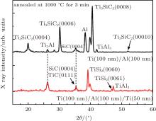 | Fig. 6. XRD spectra of the Ti/Al based contacts with different stacking species after annealing at 1000 ° C for 3 min. |
For the annealed Ti(100 nm)/Al(100 nm)/Ti(50 nm) triplelayer without a clear alloying morphology, its XRD curve is dominated by a TiSi2 phase, with Ti– Al alloy consisting of a relatively strong Ti3Al peak and also a weak TiAl3 peak. However, from the test spectra, no Ti3SiC2 is present even though it has a considerably low formation energy compared with other phases such as TiAl3.[9] This suggests that the formation of the textured Ti3SiC2 at the interface, which is responsible for the ohmic behavior of the contact after annealing, depends on the amount of liquid alloy in close proximity to the SiC surface. TiC may overlap with the SiC(0004) peak, which has commonly been found in the solid-phase reaction system having thick Ti at the interface due to the diffusion of dissociated carbon into the Ti layer.[33] Note that in both contact cases some metallic phases (e.g., 2θ ≈ 39.8° ) have also been observed but could not be positively identified using the database.
Hereafter, the contact metals are aggressively etched off with chemical reagents in the following sequence: dipping in heated aqua regia, heated potassium hydroxide solution, seven-up solution, and HF:HNO3 (1:3) solution using an ultrasonic bath. The purpose of these etches is to intuitively identify the interfacial microstructure by removing any trace of metals, alloys, or metallic oxides that might be present in the contact layer. The resulting surfaces are investigated by SEM analysis as shown in Fig. 7, where the clean surface of the as-patterned SiC sample before annealing is shown as well for easy reference.
It can be seen that the etched surface of the SiC/Ti (100 nm)/Al(100 nm) contact system subjected to RTA at 1000 ° C is entirely covered with a nonuniform layer consisting of irregular-shaped flake grains with the facet plane parallel to the [11 − 20] direction of the SiC (Fig. 7(b)). Considering the fact that the Ti– Al alloy and pure Al in the alloyed contact can be effectively removed after the wet etching as mentioned above, these residual grains having a good adhesion to the SiC surface could be determined as the Ti3SiC2, the only dominant phase observed from XRD spectra, with well-known high chemical stability. Tsukimoto et al.[32] also showed a similar Ti3SiC2 layer but with larger and more regular hexagonal facet grains in annealed Ti/Al contacts (Fig. 8). This difference may be associated with the surface status of the underlying SiC epilayer during the high-temperature annealing. In fact, it is readily understood that there is a direct influence of the surface morphology of SiC on the surface morphology of the alloyed layer formed on SiC. In the present study, the conspicuous surface step-bunching is likely to be partially decomposed in the interfacial reaction of metal-SiC because of its unstable structure. As a consequence, the initial SiC surface with ordered steps shown in Fig. 7(a) would give rise to a structural evolution in comparison with that of Tsukimoto et al., which showed an unchanged SiC surface ordering after annealing probably due to a weaker epitaxial bunching based on the 8° -inclined SiC (0001) substrate, thereby facilitating the formation of a homogeneous Ti3SiC2 cover layer with ordered surface texture. It is worth noting, however, that the irregular microstructure shown in Fig. 7(b) actually has a negligible influence on the ohmic property according to the electrical investigation, suggesting that the universal cover with a substrate-like textural orientation rather than the morphology of the ternary compound might be the key to forming an ohmic contact. Also, the most important is that the severe as-grown step-bunching does not affect the formation of a continuous interfacial Ti3SiC2 layer.
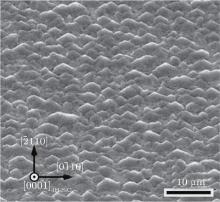 | Fig. 8. A plan-view SEM image of the Ti/Al contact deposited on p-type epilayer grown on 8° off-axis SiC(0001) substrate after 1000 ° C annealing.[32] |
On the other hand, the non-ohmic-behaved Ti(100 nm) /Al(100 nm) contact treated with RTA at 900 ° C exhibits a clean etched surface without any Ti3SiC2 grains (Fig. 7(c)). It has been reported by Pé cz et al.[34] that the Ti3SiC2 can be formed for the Ti/Al contact with the Al content of 83 at.% using the same annealing temperature but shorter annealing time (4 min). This confirms once again that the formation of Ti3SiC2 depends greatly on the liquid alloy near the interface, whether it arises from the high Al:Ti composition even at a lowered annealing temperature of 900 ° C, or at the higher annealing temperature above 1000 ° C in the case of the low Al:Ti composition used in this paper. Comparing Fig. 7(a) with Fig. 7(c) it can be seen that the original step-bunching is weakened and the steps exhibit discontinuousness, which bears out the thermal instability of the step-bunching due to the intimate contact between metal and SiC, inducing an enhanced outdiffusion of dissociated C and Si atoms even though there is no obvious alloying process at the interface.
For the annealed Ti(100 nm)/Al(100 nm)/Ti(50 nm) contact, the SEM image of the etched surface as can be seen in Fig. 7(d) clearly shows that there is a visible evidence of moderate interfacial reaction, with the existence of discrete pits and nanoparticles accompanied by disordered step arrays, however, with the exception of the Ti3SiC2 layer. This interface morphology matches well with the aforementioned optic investigation of the as-annealed contact surface, consistently pointing out that the higher the alloying degree of the layered contact during annealing is, the higher the extent of the interfacial reaction is, consequently the better the ohmic contact property is. This inference, in turn, can explain why the triple layer contact subjected to a higher annealing temperature has better I– V characteristics in terms of the quasi-linearity of the curve shown in Fig. 3(d) when compared with the bilayer contact upon the lower-temperature annealing.
In this paper, an excellent Ti/Al based ohmic contact with low SCR comparable to the level obtained from the state-of-the-art SCR is first reported on the highly doped p-type 4H-SiC epitaxial layer with a severe step-bunching surface. All investigated contact schemes are based on a low Al:Ti composition ratio with no more than 50 at.% Al, aiming at avoiding a rough contact morphology. A very low SCR of 2.6 × 10− 6 Ω · cm2 is obtained for the bilayered Ti(100 nm)/Al(100 nm) contact annealed at 1000 ° C for 3 min, while non-ohmic behavior is found when reducing the annealing temperature, i.e., Ti(100 nm)/Al(100 nm) bilayer annealed at 900 ° C for 5 min, or when adding an additional Ti layer to form a sandwich structure, i.e., Ti(100 nm)/Al(100 nm)/Ti(50 nm) triplelayer annealed at 1000 ° C for 3 min. The annealed microstructures are physically (optics, XRD) and chemical-physically (‘ chemical etching’ -assisted SEM) characterized, and the resulting evidence strongly denotes the alloying of the contact metals as the foundation of the ohmic contact formation. With the existence of intense alloying, a continuous ternary Ti3SiC2 layer is formed at the interface, responsibly leading to the ohmic behavior of annealed Ti/Al based contacts. In particular, the results reveal that the morphology of surface step-bunching is partially changed during metallization annealing, which yet has little influence on the formation of a global coverage of the textured Ti3SiC2 layer.
| 1 |
|
| 2 |
|
| 3 |
|
| 4 |
|
| 5 |
|
| 6 |
|
| 7 |
|
| 8 |
|
| 9 |
|
| 10 |
|
| 11 |
|
| 12 |
|
| 13 |
|
| 14 |
|
| 15 |
|
| 16 |
|
| 17 |
|
| 18 |
|
| 19 |
|
| 20 |
|
| 21 |
|
| 22 |
|
| 23 |
|
| 24 |
|
| 25 |
|
| 26 |
|
| 27 |
|
| 28 |
|
| 29 |
|
| 30 |
|
| 31 |
|
| 32 |
|
| 33 |
|
| 34 |
|


