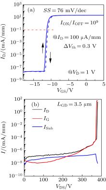
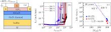
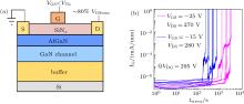
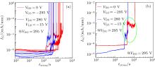
中国物理B ›› 2020, Vol. 29 ›› Issue (10): 107201-.doi: 10.1088/1674-1056/abaed8

• • 上一篇    下一篇

Tao-Tao Que(阙陶陶)1, Ya-Wen Zhao(赵亚文)1, Qiu-Ling Qiu(丘秋凌)1, Liu-An Li(李柳暗)1, Liang He(何亮)2, Jin-Wei Zhang(张津玮)1, Chen-Liang Feng(冯辰亮)1, Zhen-Xing Liu(刘振兴)1, Qian-Shu Wu(吴千树)1, Jia Chen(陈佳)1, Cheng-Lang Li(黎城朗)1, Qi Zhang(张琦)1, Yun-Liang Rao(饶运良)1, Zhi-Yuan He(贺致远)3, Yang Liu(刘扬)1,†()   

  • 收稿日期:2020-07-03 修回日期:2020-08-10 接受日期:2020-08-13 出版日期:2020-10-05 发布日期:2020-10-05
  • 通讯作者: Yang Liu(刘扬)

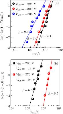
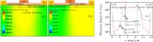
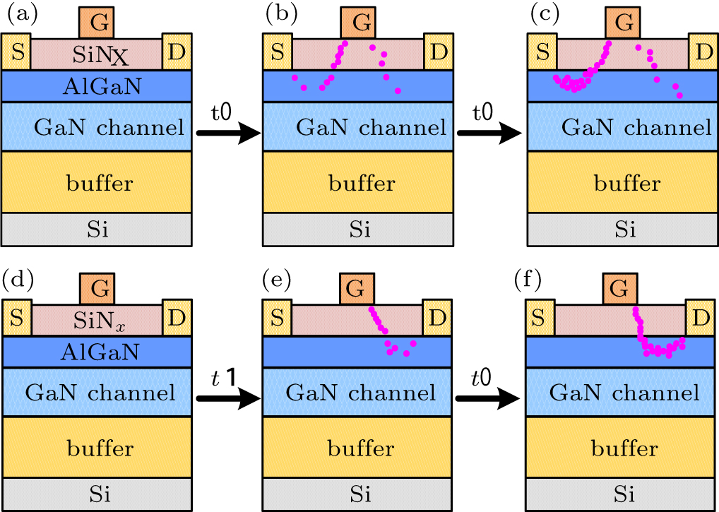
Evaluation of stress voltage on off-state time-dependent breakdown for GaN MIS-HEMT with SiNx gate dielectric

Tao-Tao Que(阙陶陶)1, Ya-Wen Zhao(赵亚文)1, Qiu-Ling Qiu(丘秋凌)1, Liu-An Li(李柳暗)1, Liang He(何亮)2, Jin-Wei Zhang(张津玮)1, Chen-Liang Feng(冯辰亮)1, Zhen-Xing Liu(刘振兴)1, Qian-Shu Wu(吴千树)1, Jia Chen(陈佳)1, Cheng-Lang Li(黎城朗)1, Qi Zhang(张琦)1, Yun-Liang Rao(饶运良)1, Zhi-Yuan He(贺致远)3, and Yang Liu (刘扬)1,†   

  1. 1 School of Electronics and Information Technology, Sun Yat-Sen University, Guangzhou 510275, China
    2 School of Materials Science and Engineering, Sun Yat-Sen University, Guangzhou 510275, China
    3 Science and Technology on Reliability Physics and Application of Electronic Component Laboratory, No. 5 Electronics Research Institute of the Ministry of Industry and Information Technology, Guangzhou 510610, China
  • Received:2020-07-03 Revised:2020-08-10 Accepted:2020-08-13 Online:2020-10-05 Published:2020-10-05
  • Contact: Corresponding author. E-mail: liuy69@mail.sysu.edu.cn
  • About author:
    †Corresponding author. E-mail: liuy69@mail.sysu.edu.cn
    * Project supported by the National Key Research and Development Program, China (Grant No. 2017YFB0402800), the Key Research and Development Program of Guangdong Province, China (Grant Nos. 2019B010128002 and 2020B010173001), the National Natural Science Foundation of China (Grant No. U1601210), the Natural Science Foundation of Guangdong Province, China (Grant No. 2015A030312011), the Open Project of Key Laboratory of Microelectronic Devices and Integrated Technology (Grant No. 202006), the Science and Technology Plan of Guangdong Province, China (Grant No. 2017B010112002), and the China Postdoctoral Science Foundation (Grant No. 2019M663233).

Abstract:

Stress voltages on time-dependent breakdown characteristics of GaN MIS-HEMTs during negative gate bias stress (with VGS < 0, VD = VS = 0) and off-state stress (VG < VTh, VDS > 0, VS = 0) are investigated. For negative bias stress, the breakdown time distribution (β) decreases with the increasing negative gate voltage, while β is larger for higher drain voltage at off-state stress. Two humps in the time-dependent gate leakage occurred under both breakdown conditions, which can be ascribed to the dielectric breakdown triggered earlier and followed by the GaN layer breakdown. Combining the electric distribution from simulation and long-term monitoring of electric parameter, the peak electric fields under the gate edges at source and drain sides are confirmed as the main formation locations for per-location paths during negative gate voltage stress and off-state stress, respectively.

Key words: gallium nitride, LPCVD-SiNx MIS-HEMT, time-dependent breakdown, negative gate bias, offstate stress

中图分类号:  (III-V and II-VI semiconductors)

  • 72.80.Ey
72.80.Sk (Insulators) 73.20.At (Surface states, band structure, electron density of states) 77.22.Jp (Dielectric breakdown and space-charge effects)