Fabrication and characterization of vertical GaN Schottky barrier diodes with boron-implanted termination
Wang Wei-Fan1, 2, Wang Jian-Feng1, 2, 3, †, Zhang Yu-Min2, 3, Li Teng-Kun1, 2, Xiong Rui2, Xu Ke1, 2, 3, ‡
School of Nano-Tech and Nano-Bionics, University of Science and Technology of China, Hefei 230026, China
Suzhou Institute of Nano-Tech and Nano-Bionics, Chinese Academy of Sciences, Suzhou 215123, China
Suzhou Nanowin Science and Technology Co., Ltd., Suzhou 215123, China


† Corresponding author. E-mail: jfwang2006@sinano.ac.cn kxu2006@sinano.ac.cn

Project supported by the National Key R&D Program of China (Grant No. 2017YFB0404100) and Science and Technology Planning Project of Guangdong Province, China (Grant No. 2017B010112001).

Abstract

The vertical GaN-on-GaN Schottky barrier diode with boron-implanted termination was fabricated and characterized. Compared with the Schottky barrier diode (SBD) without boron-implanted termination, this SBD effectively improved the breakdown voltage from 189 V to 585 V and significantly reduced the reverse leakage current by 105 times. In addition, a high Ion/Ioff ratio of ∼108 was achieved by the boron-implanted technology. We used Technology Computer Aided Design (TCAD) to analyze reasons for the improved performance of the SBD with boron-implanted termination. The improved performance of diodes may be attributed to that B+ could confine free carriers to suppress electron field crowding at the edge of the diode, which could improve the breakdown voltage and suppress the reverse leakage current.

1. Introduction

Wide bandgap materials have received increasing attention in the research and development of power electronic devices for energy conversion.[13] Gallium nitride (GaN) is a promising candidate material due to its large bandgap, high electron mobility, and high breakdown electric field.[4,5] In particular, vertical GaN power devices using GaN on GaN substrate materials with a low dislocation density (∼ 106 cm−2) are greatly developed. For example, p–n diodes (PNDs) with breakdown voltage (Vb) over 4 kV[6] and transistors with normally-off operation were well demonstrated.[7,8]

Compared with PNDs, Schottky barrier diodes (SBDs) have low turn-on voltage (Von) and fast switching. Therefore, Schottky barrier diodes have significant applications in the field of high frequency and high power devices.[9] However, SBDs typically suffer from large reverse leakage current due to the Schottky barrier lowering at high reverse biases. To suppress the reverse leakage current, advanced device structures, such as junction barrier Schottky diodes, have been well demonstrated in SiC.[10,11] But this technology is difficult to achieve in vertical GaN devices owing to the great challenge in selective Mg-implantation and activation.[12] Several methods have been used to suppress the edge leakage current and increase Vb in vertical GaN SBDs, especially including field plates with a deep trench[13,14] and a high-resistivity region around the device edge using ion implantation which can create deep-level traps.[15] What is more, introducing ions in the edge termination, which can compensate free carriers, is a common method to increase the performance of the vertical GaN power devices.[16]

There already have been a lot of reports on SiC power devices with boron-implanted technology, such as boron-implanted edge termination for 4H-SiC Schottky rectifiers and boron related deep centers caused by ions implantation in 6H-SiC.[1719] Moreover, there have been some reports about GaN vertical-cavity surface-emitting diodes and GaN MOSFETs with boron ions implantation technology.[2022] However, there are few reports about vertical GaN-on-GaN SBDs with boron-implanted technology.

In this work, we fabricated a vertical GaN-on-GaN SBD with the B+-implanted termination (BIT). Diodes with and without the BIT were characterized. The diode without the BIT is broken down at 189 V, its Schottky barrier height is 0.68 eV and its Ion/Ioff ratio is ∼ 105. Compared with the GaN SBD without B+ implanted termination technology, this SBD with the BIT has 105 × reverse leakage reduction and enhances the breakdown voltage up to ∼ 585 V. Furthermore, the SBD with the BIT obtains a high Ion/Ioff ratio of 108 and the Schottky barrier height (SBH) of 0.82 eV. This improved performance of the diode may be attributed to that B+ could confine free carriers at the edge of the diode.[20,21]

2. Experiments

Vertical GaN SBDs were fabricated on bulk GaN substrate materials. Figure 1(a) shows the schematic structures of the vertical GaN SBDs with and without the BIT, where the 6.9-μm thick n GaN homoepitaxial layer was grown by metal-organic chemical vapor deposition (MOCVD) on a free-standing n+ GaN substrate with a Si-doping concentration of ∼ 1 × 1018 cm−3. The crystal quality of the GaN epilayer was characterized by high-resolution x-ray diffraction (HRXRD) and cathodoluminescence (CL). Figure 1(b) shows the x-ray rocking curve measurements which were carried out for the symmetric (002) plane and asymmetric (102) plane. The GaN epilayer showed the full widths at half maximum (FWHMs) of 44.3 arcsec and 49.9 arcsec for the (002) and (102) planes, which indicates a dislocation density on the order of 106 cm−2. Figure 1(c) shows the plane-section CL spectrum which indicates that the threading dislocation density in the GaN epilayer is on the order of 106 cm−2. These measurements show that the dislocation density in the GaN epilayer is about ∼ 106 cm−2. Moreover, the background concentration was measured by secondary ion mass spectroscopy (SIMS) as shown in Fig. 2(a). The concentration of Si impurities is about 2.5 × 1016 cm−3 and the concentration of C, H, and O impurities is close to the detection limit, which indicates that the background concentration in the GaN epilayer is very low. The surface morphology of the GaN epilayer was characterized by atomic force microscopy (AFM) as shown in Fig. 2(b). The root-mean-square (RMS) roughness of a 10 μm × 10 μm scanning area of the GaN epilayer is 0.20 nm. These characterization results show the high crystal quality and smooth surface of the GaN epilayer with low background concentration.
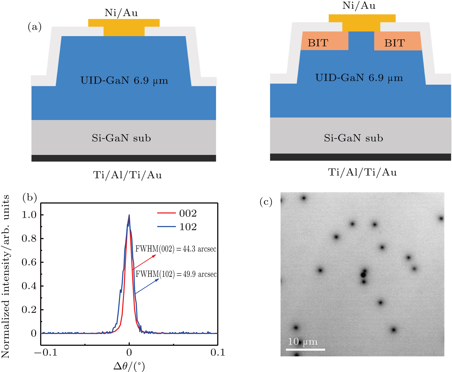
Fig. 1. (a) The schematic structures of the vertical GaN-on-GaN SBDs with and without the BIT. (b) Rocking curves of the (002) and (102) planes of the GaN epilayer. (c) The plane-section CL image.
Fig. 2. (a) The concentration of C, H, O, and Si in GaN-on-GaN MOCVD growths by SIMS. (b) The AFM image of the epilayer in a range of 10 μm × 10 μm.

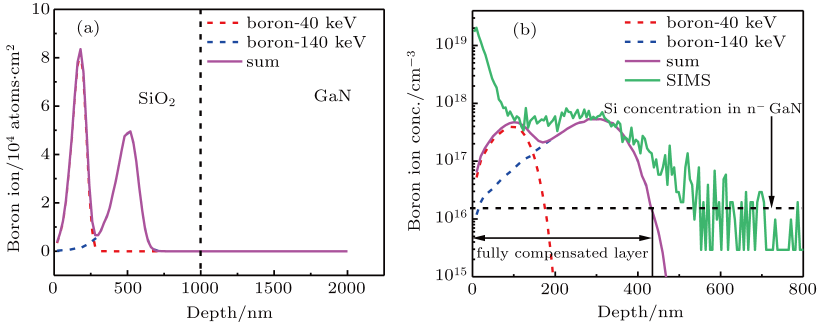
The device fabrication started with 1-μm deep mesa isolation etch by inductively coupled plasma (ICP). Then 1-μm thick SiO2 was deposited by plasma-enhanced chemical vapor deposition (PECVD), followed by selectively etching of SiO2 to form a hard mask for the next ion implantation. As shown in Fig. 3(a), the distribution of boron ions in the 1-μm thick SiO2 at 40 keV and 140 keV implantation energy was simulated by SRIM (stopping and range of ions in matter). It shows that boron ions are mainly distributed within 750 nm in SiO2, which means that 1-μm thick SiO2 as a hard mask can protect the active area during boron ions implantation. The BIT structure was formed by B+ implantation at two energy levels of 40 keV and 140 keV with doses of 0.4 × 10¹³ at./cm2 and 1.0 × 10¹³ at./cm2, respectively. Figure 3(b) shows the B+ distribution inside the sample for the ion energy of 40 keV and 140 keV simulated by SRIM. The distribution of B+ measured by SIMS was the same as the result simulated by SRIM in Fig. 3(b). After implantation and SiO2 removal, a 100-nm thick SiO2 was deposited on the GaN epilayer by PECVD. Next, rapid thermal annealing was carried out at 450 °C in N2 atmosphere for 10 min to recover the damage caused by the ions implantation.[23] Then we selectively etched off SiO2 to form the field plates (FPs) by BOE solution. Afterward, a Ni/Au (40 nm/200 nm) metal stack was deposited on a pre-cleaned GaN surface by e-beam evaporation as the anode and patterned by lift-off. Finally, the N-face was treated by ICP in order to introduce nitrogen vacancies[2426] and a Ti/Al/Ti/Au (20 nm/130 nm/50 nm/150 nm) metal stack was deposited by e-beam evaporation to form an Ohmic contact to the backside of the n+ GaN substrate. In the meantime, diodes without the BIT were fabricated for the reference.

Fig. 3. (a) The distribution of boron ions in 1-μm thick SiO2 at 40 keV and 140 keV implantation energy simulated by SRIM. (b) The distribution of boron ions in GaN simulated by SRIM at 40 keV and 140 keV implantation energy and measured by SIMS.
3. Results and discussion

Figure 4 shows the capacitance–voltage (CV) and 1/C2V characteristics of the device drift layer at a frequency of 500 kHz. As shown in Fig. 4(b), the net carrier concentration (NDNA) can be calculated as[27]

where A is the effective area of the diode (200 μm in diameter), q is the electron charge, ε0 is the permittivity of the vacuum, and εr is the relative permittivity of GaN. The net carrier concentration of the unintentionally doped GaN drift layer is ∼ 1.06 × 1016 cm−3, which comes from the background of MOCVD reactants.

Fig. 4. (a) The CV characteristic of the device drift layer. (b) The extracted free carrier concentration in the device drift layer.

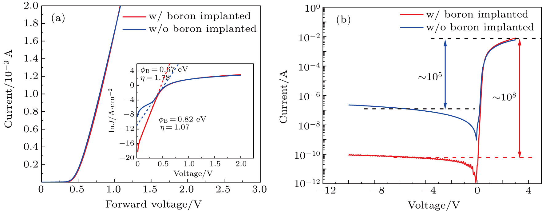
Figure 5(a) presents the forward current–voltage (IV) curves of the GaN-on-GaN SBDs. The devices with and without the BIT show comparable IV curves at forward voltage, indicating that the B+-implanted treatment does not obviously degrade the forward IV characteristic of the diode.

Fig. 5. (a) Forward characteristics of the diodes with and without the BIT. Inset: ln(J) as a function of V. (b) The IV characteristics of the diodes with and without the BIT.

Table 1 summarizes the forward IV characterization for the diodes with and without the BIT. The Von of the diodes with and without the BIT that were extracted from the forward IV curves are 0.49 V and 0.51 V, respectively. The on-resistances (Ron) of the diodes with and without the BIT are 71.2 mΩ⋅cm2 and 68.8 mΩ⋅cm2, respectively. Besides, we extracted the Schottky barrier height (SBH) and ideality factor (η) from the forward IV curves that are shown in the inset of Fig. 5(a) by using the thermionic emission model[28]

where J is the current density, A* is the Richardson constant (26.4 cm−2⋅K−2 for GaN), T is the thermodynamic temperature, k is the Boltzmann’s constant, η is the ideality factor, and φB is the Schottky barrier height. From Table 1, the diode without the BIT has a low SBH (0.68 eV) and the ideality factor (1.78) is larger than 1.00, which mean that the diode presents the trap/defect related leakage and recombination currents.[29,30] Compared to the diode without the BIT, the BIT-diode has a higher SBH (0.82 eV) and the ideality factor (1.07) is close to 1.00. The BIT-diode has a higher Ion/Ioff ratio in the order of 108 as shown in Fig. 5(b).

Table 1.

Comparison of forward characteristics of the diodes with and without the BIT.

.

Figure 6(a) shows the reverse characteristics of the diodes with and without the BIT. The breakdown voltage of the diode with the BIT is 585 V while that of the diode without the BIT is 189 V. What is more, the reverse leakage current is reduced by five orders of magnitude by using the boron-implanted technology at 100 V.

Fig. 6. (a) Reverse IV characteristics of the diodes with and without the BIT. (b) Simulated electric field distributions in the diodes without the BIT (left) and with the BIT (right) at −600 V.

The above results show that the B+-implanted termination technology could improve the performance of vertical GaN-on-GaN SBDs such as breakdown voltage and reverse leakage current. The reason why the BIT structure could improve the performance of the diodes is that B+ could confine free carriers in the GaN drift layer. As shown in Fig. 3(b), the concentration of B+ implanted measured by SIMS is above the order of 1017 cm−3, which is much greater than the net doping concentration measured by CV. Therefore, we assume that the free carriers in the B+-implanted region are fully compensated in TCAD simulation. TCAD simulations solve the Poisson equation and the electron and hole current continuity equations to predict the behavior of semiconductor devices under electrical stress as follows:

where εs is the semiconductor permittivity, ϕ is the electrostatic potential, q is the electron charge, n and p are the free electron and hole densities, is the ionized donor density, is the ionized acceptor density, Jn/p is the electron and hole current density, Gn/p is the rate of regeneration for electrons and holes, and Rn/p is the rate of recombination for electrons and holes. Besides, some special models such as field dependent mobility (FLDMOB), Shockley–Read–Hall (SRH), and Auger recombination (Auger) are used to simulate the Schottky diode. As shown in Fig. 6(b), the diode without the BIT presents severe electric field blocking effects at the edge of the diode where the electric field is higher than the critical breakdown electric field of GaN (3.75 MV/cm).[15] Compared to the diode without the BIT, the electric field distribution is uniform in the BIT-diode and the electric field crowding effects at the edge of the diode can be effectively suppressed where the free carriers are fully compensated, which could increase the breakdown voltage of the diodes and reduce the reverse leakage current.

4. Conclusion

We fabricated and characterized vertical GaN-on-GaN Schottky barrier diodes with and without boron-implanted termination. The Schottky barrier height in the diode with the BIT was 0.82 eV and the ideality factor was 1.07. Compared to the diode without the BIT, the breakdown voltage was improved from 189 V to 585 V, the Ion/Ioff ratio was in the order of 108, and the reverse leakage current was reduced by five orders of magnitude. The condition parameters of B+ implantation were simulated by SRIM. And we attributed the improved performance of the diode with the BIT to boron ion confining free carriers at the edge of the diode. From TCAD simulation results, the electric field crowding effect at the boundary of the diode with the BIT was suppressed, which could improve the breakdown voltage and suppress the reverse leakage current. Therefore, the boron ions implantation technology shows great potential for vertical GaN-on-GaN power devices as the termination structure.

Reference
[1] Pearton S J Ren F 2000 Adv. Mater. 12 1571
[2] Yong C Yugang Z Chen K J Lau K M 2005 IEEE Electron Device Lett. 26 435
[3] Wang M J Yuan L Chen K J Xu F J Shen B 2009 J. Appl. Phys. 105 083519
[4] Ueda T 2014 International Power Electronics Conference (IPEC-Hiroshima 2014-ECCE ASIA) May 18–21, 2014 Hiroshima, Japan 2075 2078 10.1109/IPEC.2014.6869874
[5] Mishra U K Shen L Kazior T E Wu Y F 2008 Proc. IEEE 96 287
[6] Kizilyalli I C Prunty T Aktas O 2015 IEEE Electron Device Lett. 36 1073
[7] Wang M Chen K J 2011 IEEE Trans. Electron. Devices 58 460
[8] Tapajna M Hilt O Bahat-Treidel E Wurfl J Kuzmik J 2016 IEEE Electron Device Lett. 37 385
[9] Yang S Han S Li R Sheng K 2018 IEEE 30th International Symposium on Power Semiconductor Devices and ICs (ISPSD) May 13–17, 2018 Chicago, IL, USA 272 275 10.1109/ISPSD.2018.8393655
[10] Bolotnikov A V Muzykov P G Zhang Q Agarwal A K Sudarshan T S 2010 IEEE Trans. Electron. Devices 57 1930
[11] Sung W Van Brunt E Baliga B J Huang A Q 2011 IEEE Electron Device Lett. 32 880
[12] Zhang Y Liu Z Tadjer M J Sun M Piedra D Hatem C Anderson T J Luna L E Nath A Koehler A D Okumura H Hu J Zhang X Gao X Feigelson B N Hobart K D Palacios T 2017 IEEE Electron Device Lett. 38 1097
[13] Tanaka N Hasegawa K Yasunishi K Murakami N Oka T 2015 Appl. Phys. Express 8 071001
[14] Saitoh Y Sumiyoshi K Okada M Horii T Miyazaki T Shiomi H Ueno M Katayama K Kiyama M Nakamura T 2010 Appl. Phys. Express 3 081001
[15] Ozbek A M Baliga B J 2011 IEEE Electron Device Lett. 32 300
[16] Wang J Cao L Xie J Beam E McCarthy R Youtsey C Fay P 2018 Appl. Phys. Lett. 113 023502
[17] Addamiano A Anderson G W Comas J Hughes H L Lucke W 1972 J. Electrochem. Soc. 119 1355
[18] Itoh A Kimoto T Matsunami H 1996 IEEE Electron Device Lett. 17 139
[19] Suttrop W Pensl G Lanig P 1990 Appl. Phys. 51 231
[20] Hamaguchi T Nakajima H Ito M Mitomo J Satou S Fuutagawa N Narui H 2016 Jpn. J. Appl. Phys. 55 122101
[21] Jiang Y Wang Q P Tamai K Li L A Shinkai S Miyashita T Motoyama S I Wang D J Ao J P Ohno Y 2014 Semicond. Sci. Technol. 29 055002
[22] Jiang Y Wang Q Zhang F Li L Shinkai S Wang D Ao J P 2016 Semicond. Sci. Technol. 31 035019
[23] Taube A Kamińska E Kozubal M Kaczmarski J Wojtasiak W Jasiński J Borysiewicz M A Ekielski M Juchniewicz M Grochowski J Myśliwiec M Dynowska E Barcz A Prystawko P Zajac M Kucharski R Piotrowska A 2015 Physica Status Solidi (a) 212 1162
[24] Jeon J W Park S H Jung S Y Lee S Y Moon J Song J O Seong T Y 2010 Appl. Phys. Lett. 97 092103
[25] Jang J S Kim D Seong T Y 2006 J. Appl. Phys. 99 073704
[26] Boguslawski P Briggs E L Bernholc J 1995 Phys. Rev. B Condens Matter 51 17255
[27] Fu H Baranowski I Huang X Chen H Lu Z Montes J Zhang X Zhao Y 2017 IEEE Electron Device Lett. 38 1286
[28] Schroder D K 2005 Semiconductor material and device characterization New York John Wiley & Sons 129 133 10.1002/0471749095
[29] Hu Z Nomoto K Song B Zhu M Qi M Pan M Gao X Protasenko V Jena D Xing H G 2015 Appl. Phys. Lett. 107 243501
[30] Suzue K Mohammad S N Fan Z F Kim W Aktas O Botchkarev A E Morkoç H 1996 J. Appl. Phys. 80 4467