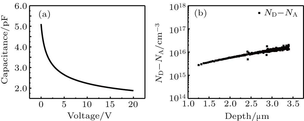
Fabrication and characterization of vertical GaN Schottky barrier diodes with boron-implanted termination
Wang Wei-Fan1, 2, Wang Jian-Feng1, 2, 3, †, Zhang Yu-Min2, 3, Li Teng-Kun1, 2, Xiong Rui2, Xu Ke1, 2, 3, ‡
       

(a) The CV characteristic of the device drift layer. (b) The extracted free carrier concentration in the device drift layer.