Fabrication and characterization of vertical GaN Schottky barrier diodes with boron-implanted termination
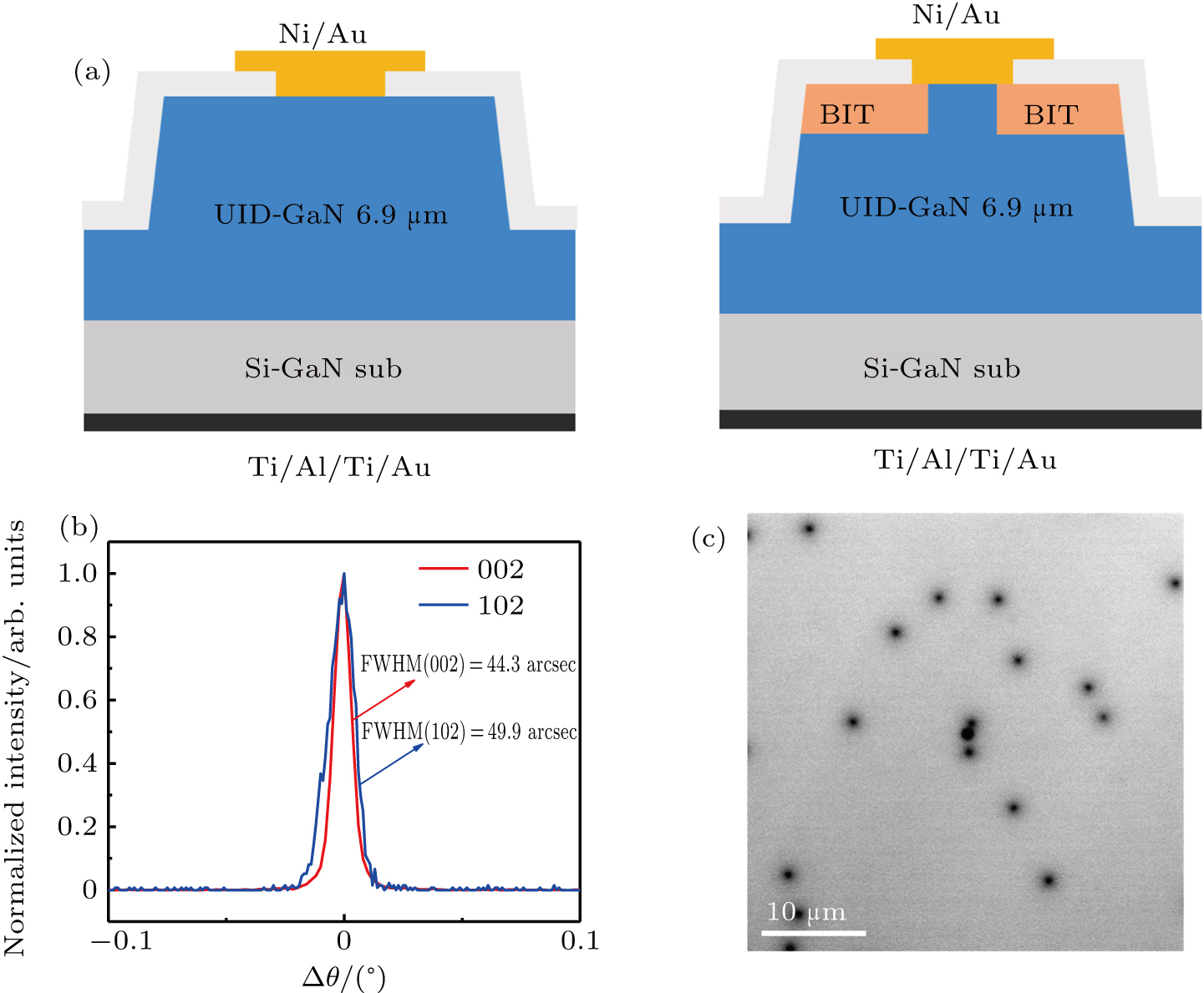
(a) The schematic structures of the vertical GaN-on-GaN SBDs with and without the BIT. (b) Rocking curves of the (002) and (102) planes of the GaN epilayer. (c) The plane-section CL image.