1. IntroductionSi thin or ultrathin crystals are crucial in applications such as flexible solar cells, silicon-on-insulator (SOI), flexible integrated circuit (IC) chips, insulated gate bipolar transistor (IGBT), etc.[1–8] In order to avoid kerf loss during Si wafer thinning process that has frustrated people for years, kerfless technology is eagerly demanded. On the one hand, kerfless technology can reduce about 30% of the total cost in slicing process in which a traditional Czochralski method is used;[9,10] on the other hand, thin/ultrathin and flexible silicon crystals are readily available by epitaxial growth and transfer approaches directly. Double layer porous silicon method, one of the kerfless techniques,[11,12] is capable of preparing kerfless flexible Si thin crystals with good properties. However, limited reuse times of the substrate and metal contaminants from electrochemical electrodes restrict its wide industrial applications.
In our team’s previous research, the patterned rod arrays with wax acting as the filling mask provided protruded Si seeds by removing the oxide layer on the heads of the patterned rods, and the epi-Si film/wafer grown on them had texturized surface with the same periodicity as the original rod pattern. The uniformly structured hollows have been built between the epi-Si film and the substrate so that the epi-Si film could be transferred without sacrificing any layer, thereby making the substrate reusable.[13] Due to the difficulty in using wax to form uniform and flat thin films, only long rod arrays are applicable to fabricating the seeded substrates with wax used as filling mask. In order to enhance the mechanical stability of the seed structure and increase the reuse possibility of the structured substrate, short rods would be preferred. Later, efforts had been made to fabricate seeded substrates with shorter rod arrays by a joint resist mask method.[14] Thermal evaporation deposited aluminum film, spin-coated poly methyl methacrylate (PMMA) and photoresist were used to form the joint mask. Protruded seed substrate was achieved by removing the oxide layer selectively from the rod heads under the masking effect of the joint mask. However, multiple filling and etching process were involved in the joint mask method, and the processing is complicated and boring.
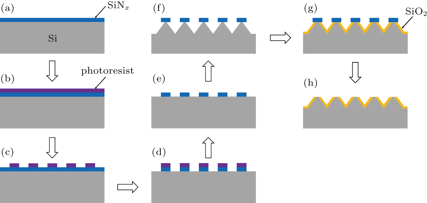
In this article, we demonstrate a simple and low-cost approach to preparing mechanically stable wedge-grooved seed substrates with SiNx thin film serving as the mask layer for wet-etching and thermal oxidation without expensive inductive coupled plasma dry-etching process.[15,16] The vapor phase epitaxial growing process is implemented to produce epi-Si on this substrate by using gaseous SiCl4 as a silicon source.[17] An intermittent silicon-source-feeding technique is used to control the preferred growth behavior on the seed sites and well-faceted growth is successfully performed. The endeavors shown in this work will promote the development of kerfless technology for further industrial applications.
3. Results and discussionThe morphology of the obtained grooved seed Si substrate and energy dispersive spectrum (EDS) analysis are shown in Fig. 2. Figures 2(a) and 2(b) demonstrate that the wet-etching of the substrate has high self-discipline characteristics under the mask of SiNx stripes, and the formed strips present wedge-like shapes. The angle at the bottom of V-grooves is 70.5°, similar to the one between adjacent Si {111} planes, indicating that only Si {111} plane remains during etching process,[20] and also that the areas with SiNx masks are kept from alkaline etching, thus defining the shape and size of the grooved Si seed. In order to show up the seeded sites and prove the seed architecture, i.e., silicon surface exposed only on the top of the wedged-strips, a diluted KOH solution is used to etch the prepared seed substrates. Figure 2(c) and 2(d) reveal that shallow depressions appear on the tops of the wedged-strips, indicating the etching has happened here by KOH solution, but other surface on the seed substrate is protected from visibly etching. This phenomenon made it clear that the silicon surface is exposed just on the tops of the wedged-strips and the other surface of the substrate is sheathed. The EDS spectra further prove the architecture of the seed substrate. As shown in Fig. 2(e), the SiNx layer stands on the top of the wedged-strip and a pure silicon surface is exhibited on the V-grooves after the KOH wet etching of the original silicon substrate under the mask of striped SiNx film, but after the procedures of thermal oxidization and removal of the left SiNx on the strip top, pure silicon surface is exposed on the strip top and the grooves are sheathed by oxide layers. As a result, the seeded substrates are well-built and ready to be used for the epi-Si growth.
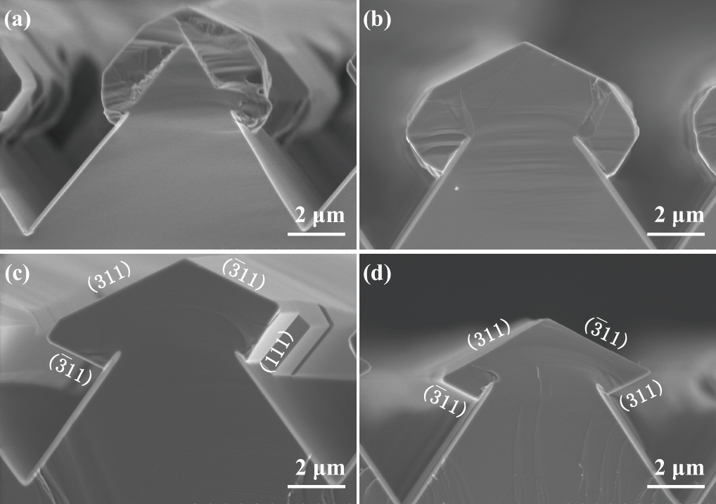
Figure 3 illustrates the morphologies of epi-Si grown on the substrate. Epi-Si grown in the uninterrupted mode is shown in Fig. 3(a), it appears that the shape of the grown epi-Si is irregular, and although the epitaxial growth is preferred on the seeded sites, a fast lateral overgrowth also occurs downward along the slopes of the V-grooves. It is inferred that the fast downward lateral growth results from the high supersaturation of silicon tetrachloride that migrates from the V-groove surface to the interface between the grown silicon and the oxide layer, and the irregular shape of the grown silicon rises from the reverse etch reaction of by-product chlorides on the silicon surface because the concentration of by-product chlorides in the chamber is accumulated with the growth duration increasing. In order to achieve well-faceted surface and enhance the anisotropic growth over the groove, the intermittent source gas feeding method is adopted.[21–23] The morphology evolutions of the epi-Si with the silicon source feed mode are demonstrated in Figs. 3(a)–3(d). Obviously, the grown epi-Si becomes better faceted and larger over the groove with the faster repetition rate of SiCl4 on-and-off feeding, as well with shorter on-and-off intervals, from Figs. 3(a)–3(d). Additionally, the size of grown Si does not vary much in Fig. 3(b) nor in Fig. 3(c) compared with that in Fig. 3(a) although the total amount of SiCl4 feeding decreases to 1/2 and 1/3 of that in Fig. 3(a) for the whole growth duration. In other words, the intermittent feed mode increases the growth rate of the epi-Si. Since the carrier gas, H2 with a light molecular weight, has a rather weak carrying capability under the atmosphere pressure, the concentration of chloride byproduct, such as HCl, from the reduction reaction between SiCl4 and H2, would accumulate around the substrate holder zone with the growth duration increasing. It is understandable that the intermittent feed mode would restrain the byproduct accumulation. Thus the conversion rate of SiCl4 into Si is promoted as can be seen from Figs. 3(a)–3(c), and less reverse etch reaction on the grown Si results in better faceted surfaces.
According to the intersection angles between faceted surfaces of the grown Si and the grooves, the surface planes of the grown Si are indexed in Figs. 3(c) and 3(d). It is revealed that the front side surfaces facing the gas flow are indexed to {311} both in Fig. 3(c) and in Fig. 3(d), but for the back side surfaces against the gas flow, one is indexed to {111}, the other is indexed to {311} in Fig. 3(c); contrastively, both back surfaces are symmetrically indexed to {311} in Fig. 3(d). Si crystal belongs to the cubic crystal system with the two-fold symmetry along the
 direction. Bravais–Friedel law states that high index crystal planes with small interplanar spacings grow faster than the low index ones, and thus the high index planes are not seen in the final shape of the crystal.[24] Therefore, from the point of crystallographic growth habit, the shape of the crystal is determined by the relative growth rate at various crystal planes. Si crystal belongs to the cubic crystal system with the two-fold symmetry along the
 direction. In the case of
 crystallographic direction family in the cubic crystal system, the lowest index plane belongs to {111} and the second lowest one is {311}. Therefore, considering both the crystallographic growth habit and the symmetry, the surface planes of the grown Si bars along the
 direction are surely adjacent {111}, {311} planes, or parallel ones. Undoubtedly, the situation in Figs. 3(c) and 3(d) confirm the above theoretical analysis. Owing to the higher supersaturation of reactants on the surface facing the gas flow, the front surfaces are energetically apt to be {311} planes both in Fig. 3(c) and in Fig. 3(d). On account of the shelter effect from the grown Si bars, less reactants can reach the back surfaces of the grown bars, and lower supersaturation of reactants on the back surface against the gas flow should energetically result in {111} back planes both in Fig. 3(c) and in Fig. 3(d) because {111} planes have lower surface-energy state than {311} planes. It is thought that the feed of 12-sccm SiCl4 in Fig. 3(d) is too small to provide enough reactants to form lower-energy state {111} planes on the back of the grown bars, thus two higher-energy state {311} planes are left behind there. Owing to the non-uniformity of the gas flow distribution in the chamber, even though the feed amount of SiCl4 in Fig. 3(c) is double that in Fig. 3(d), one of the back-surface planes belongs to {111}, the other still belongs to {311}.
In order to obtain a faster growth rate and well-faceted surfaces of the grown Si bars, the growth conditions in Fig. 3(c) are used as the optimized ones, and 1-
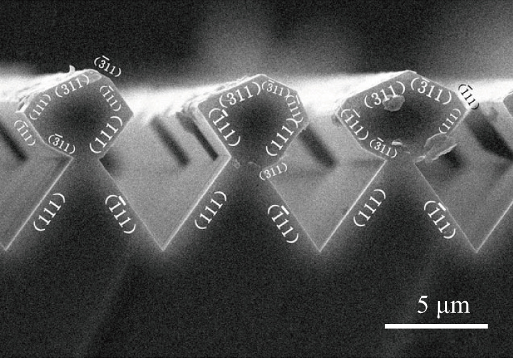
 top width of the seed stripes is chosen for narrower necks that connect the grown Si bars with the mother substrate. The typical facet profile of the grown Si bars is displayed in Fig. 4, revealing that the surface facets are step-like, and all of them are indexed to {111} and {311} planes, but the combination of {111} and {311} planes is random for each individual grown bar since the reactant flow is hard to be uniformly distributed across the substrate. Anyway, the facet profile in Fig. 4 clearly verifies the dominance of the crystallographic symmetry and the Bravais–Friedel law of the silicon seed growth.
From the point of the mass-transport in the course of epi-Si growth, the models of gas flow around the substrate are proposed in Fig. 5 to further clarify the growth mechanism on the seeded substrate. As shown in Fig. 5(a), at the initial stage of the epi-growth, there are two kinds of gas flows on the surface of the substrate, i.e., flow 1 and flow 2. The flow 1 goes straight down to the substrate while a large portion of the flow 1 is reflected by the slopes of the V grooves and turns into the turbulent flow 2, then the flow 2 is trapped and enveloped by the V grooves and the flow 1. Consequently, at the initial stage, two parts of silicon reactant are gathered up at the seeded sites, i.e., one is directly anchored from the flow 1 that faces the seeded areas; the other diffuses from the flow 2 along the slopes of the grooves. Thus the supersaturation of the silicon reactant is quite high and the nucleation and growth-up of silicon quickly happen on the seeds at the early stage when the SiCl4 gas is just introduced into the chamber. Once the epi-Si grows up to a size larger than the width of the seeded sites, the epi-Si will shelter the V-grooves from the flow 1, accordingly, as shown in Fig. 5(b), the curved flow 3 under the epi-Si and the parallel flow 4 at the opening of the groove come into being, and as a result, the trapped gas in the grooves turns harder to escape out. Therefore, it could be inferred that if the feed amount of SiCl4 is fairly large, much of the byproduct chloride will be trapped in the grooves, and then diffuse and accumulate around the grown epi-Si, the growth rate of the epi-Si will be inhibited by the severe reverse etch reaction, and much lateral overgrowth will happen along the slopes due to the high degree of supersaturation at the interface between the grown Si and the oxide layers (as shown in Figs. 3(a) and 5(d), and it was very necessary that intermittent SiCl4 feed mode is used to facilitate the trapped gas off the grooves. And the intermittent feed mode can help the epi-Si grow nearly under the equilibrium state, thereby well-faceted surfaces are formed (as shown in Figs. 3(c) and 3(d)). Figures 5(c) and 5(d) show the schematic facet profile of the grown Si bars under perfect equilibrium growth state, without and with lateral overgrowth along the oxide layers, respectively, but these phenomena hardly happen in actual experiments (the profile in Fig. 4 is common in experiments).
Using the intermittent feed mode in Fig. 3(c) as an optimized mode, Figure 6 shows the panorama of prepared epi-Si from just shooting out on the seed sites, subsequently growing larger and over the grooves, eventually forming continuous film with hollows spacing the substrate. Evidently, the growth of Si along the seeded stripe is uniform, although slightly terraced. And the readily formed hollows between the grown film and the substrate are shaped into a tetragon usually with two-fold symmetry, which is determined by the faceted growth habit and the preferred growth behavior. And the hollows build weak mechanical connection of grown films with the mother substrate, and will make the aimed kerfless technology practical. The surface of the grown film is randomly texturized with grooved depressions, which also results from the faceted epi-growth and the non-uniformity of the reactant flows. The epi-growth panorama on the seeded substrate verifies the principle for kerfless silicon wafers by the vapor phase epi-growth method through using V-grooved seed substrates. By the way, in the traditional Siemens method to produce the crystalline Si, the SiHCl3 is most used as a silicon source because of the higher conversion rate, the faster growth rate,[25] and the lower growth temperature than those of SiCl4, if the SiHCl3 is used in our experiments, better epi-growth and thicker films or wafers can be expected.


