

Effect of PECVD SiNx /SiOy Nx –Si interface property on surface passivation of silicon wafer
[Jia Xiao-Jie1, Zhou Chun-Lan1, †,  , Zhu Jun-Jie2, Zhou Su1, Wang Wen-Jing1]
, Zhu Jun-Jie2, Zhou Su1, Wang Wen-Jing1]
|
|


† Corresponding author. E-mail:
Project supported by the National High Technology Research and Development Program of China (Grant No. 2015AA050302) and the National Natural Science Foundation of China (Grant No. 61306076).
It is studied in this paper that the electrical characteristics of the interface between SiOyNx/SiNx stack and silicon wafer affect silicon surface passivation. The effects of precursor flow ratio and deposition temperature of the SiOyNx layer on interface parameters, such as interface state density Dit and fixed charge Qf, and the surface passivation quality of silicon are observed. Capacitance–voltage measurements reveal that inserting a thin SiOyNx layer between the SiNx and the silicon wafer can suppress Qf in the film and Dit at the interface. The positive Qf and Dit and a high surface recombination velocity in stacks are observed to increase with the introduced oxygen and minimal hydrogen in the SiOyNx film increasing. Prepared by deposition at a low temperature and a low ratio of N2O/SiH4 flow rate, the SiOyNx/SiNx stacks result in a low effective surface recombination velocity (Seff) of 6 cm/s on a p-type 1 Ω·cm–5 Ω·cm FZ silicon wafer. The positive relationship between Seff and Dit suggests that the saturation of the interface defect is the main passivation mechanism although the field-effect passivation provided by the fixed charges also make a contribution to it.
Silicon oxynitride (SiOyNx) deposited through plasma-enhanced chemical vapor deposition (PECVD) has been widely used in microelectronic and optoelectronic devices.[1] The most significant feature of SiOyNx thin film is that its composition and properties can be easily controlled by varying precursor gas-flow ratio in deposition and post-annealing process. In recent years, SiOyNx, which is usually presented in the form of SiOxNy/SiNx stacks, has shown great potential applications in various designs of the next-generation high-performance solar cells.[2] SiOyNx offers an adjustable refractive index between 1.45 and 2.1[3,4] and provides better transmission coefficient than single-layered silicon nitride (SiNx). The coefficient makes it become a multilayer antireflection coating on the front side of solar cells. Silicon solar cells become thin to reduce wafer cost; thus, there exists a stronger reliance on the surface passivation of solar cells in the efficiency of silicon solar cells. SiOyNx has a large fixed positive charge density after being annealed;[5] thus, it is an effective passivation layer for various high-performance solar cells, particularly as a rear passivation layer in passivated emitter and rear cell (PERC) solar cells.[6,7] In our previous work,[8] inserting a PECVD-deposited SiOyNx layer between the SiNx capping layer and the silicon wafer shows an increased resistance to potential-induced degradation (PID) compared with the single SiNx layer.
Thus far, extensive work has been conducted to investigate the passivation properties of SiOyNx thin films. Most of these studies are based on how the deposition parameters and the annealing methods affect the stoichiometry of thin film and influence the minority carrier lifetime. Sommer et al.[9] determined oxygen concentration increases as N2O gas dilution ratio rising, while the nitrogen remains nearly unchanged. Their observations implied that oxygen replaces hydrogen in films. This finding agreed with the report of Dupuis et al.,[10] indicating that low oxygen content sample with high hydrogen content exhibits a better surface passivation before being annealed than a sample with high oxygen content. The annealing process affects the hydrogen content in the film[11] and changes the sign of charge in the film, with a negative charge in the film before being annealed and a positive charge after being annealed.[12] However, clarifying how the electrical properties of the interface between the dielectric film and the silicon wafer affect the silicon surface passivation needs in-depth investigation.
The present study aims to examine how N2O/SiH4 gas flow ratio (R) and the deposition temperature of SiOyNx thin layer affect the SiOyNx/SiNx–stack/silicon interface and the surface passivation of silicon wafer. The interface properties are analyzed via capacitance–conductance–voltage (C–G–V) measurement and noncontact corona C–V metrology. The passivation influence of the layer is quantified through effective minority carrier lifetime measurement using quasi-static state photo-conductance (QSSPC) method.
High-quality double-side-polished 1 Ω·cm–5 Ω·cm FZ p-type silicon wafers were used as substrates. The wafers experienced a standard RCA cleaning and a 1-min oxide removal process in a 1-wt% HF solution prior to PECVD processing.
The SiOyNx films were deposited on silicon wafers in a PECVD system (PlasmaLab System133) from Oxford Instruments. Silane (SiH4) and nitrous oxide (N2O) were used as precursor gases. The microwave power and the pressure were maintained at a constant value of 47 mW/cm2 and 500 mTorr (1 Torr = 1.33322 × 10² Pa), respectively. The deposition temperature varied from 35 °C to 400 °C. The R of SiH4 and N2O flow ratio, R, was controlled from 0.44 to 77.
After the deposition of SiOyNx film, the capping layer, a 70-nm SiNx film, was deposited in the same PECVD chamber. Ammonia (NH3) and SiH4 were used as precursor gases. The microwave power, the pressure, and the deposition temperature were kept at 58 mW/cm2, 800 mTorr, and 400 °C, respectively. The refractive index of the SiNx layer, which was measured via spectroscopic ellipsometry (JobinYvon UVISEL), was 2.04 at wavelength λ = 630 nm.
After the deposition of the SiOyNx/SiNx stack structure, the rapid thermal annealing (RTA) was performed on each of the samples at approximately 800 °C for 5 s. This process imitates the co-firing screen printing of Ag and Al at the end of the production of the silicon solar cells.
Metal–insulator–semiconductor (MIS) structures were prepared to perform the C–G–V characterization. For all kinds of samples, the aluminum contact of 100 nm was thermally evaporated to produce Al/Si/SiOyNx/SiNx/Al device and Al/Si/SiNx/Al as references. The diameter of the circular gate electrode was 3 mm. Multifrequency (10 kHz to 2 MHz) C–V and G–V measurements were performed with a Keithley 4200 SCS using the parallel model.[13] All measurements were compensated for by a series resistance. The interface state density (Dit) in half the band gap could be extracted by combining the C–V and G–V tests. A noncontact C–V metrology (PV2000, Semilab) was used to investigate the energy distribution of the Dit in the band gap for post-RTA sample.[14]
The effective minority carrier lifetime (τeff) of p-type silicon wafer that was double-side coated with the SiOyNx/SiNx stacks was observed. A silicon wafer that was double-side coated with the single 100-nm-thick SiNx film was used as reference. QSSPC measurements (Sinton Instruments lifetime tester) were performed with the optical constant as “1- reflection index” at an injection level of Δn = 7 × 1014 cm-3. The effective surface recombination velocity (Seff) can be calculated from[15]

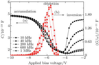
The multifrequency C–G–V characteristics of one of the post-RTA SiOxNy/SiNx stack samples are shown in Fig.
 | Fig. 1. Multifrequency (10 kHz to 1 MHz) C–G–V characteristics of an MIS capacitor utilizing post-RTA SiOyNx/SiNx stacks. (a) The C–V curves were measured in inversion–accumulation direction. (b) The peaks of G/ω–V curves lie in the range of depletion. |
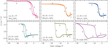
The varying N2O/SiH4 gas flow ratio (R) changes the Si, O, and N concentrations in the SiOyNx layer. The hysteresis formation of the SiOyNx (30 nm)/SiNx (70 nm) stacks is measured using inversion–accumulation–inversion complete circles as shown in Fig.
 | Fig. 2. Compositions of the SiOyNx layer of the SiOyNx (30 nm) / SiNx (70 nm) stacks influence the hysteresis in C–V curves. The complete measurement circle is inversion–accumulation–inversion. In the SiOy/SiNx stacks, (a) R = 77. In the SiOyNx/SiNxstacks, (b) R = 11.11, (c) R = 1.54, (d) R = 0.83, and (e) R = 0.54. The reference is (f) the single SiNx (100 nm) layer. |
The largest hysteresis is observed in the sample with only a single SiNx layer at ΔVFB = 13 V. For PECVD-prepared SiNx film, the hysteresis of the Si-rich film with numerous Si dangling bonds is larger than that of the N-rich film.[18] The SiOyNx films deposited with low R values of 0.44 and 0.83 each show a counter-clockwise hysteresis formation, which can be interpreted by the following hole-trapping mechanism:[19] High-density hole trapping sites possibly exist at the interface. These trapping sites can be filled with majority carrier holes at the accumulation state when voltage sweeping is applied from inversion to accumulation. Therefore, the excess positive charge trapped at the interface can make the flat voltage (VFB) shift to a negative applied bias voltage when voltage sweeping is applied from accumulation back to inversion. The VFB is affected by the applied bias sweep range and by its history, and the injected charges generate hysteresis during the C–V measurements, thereby leading to the shift of the VFB. For instance, the hysteresis effect of the single SiNx layer is reduced by inserting a SiOyNx layer at R = 0.83, thereby making the ΔVFB decrease to 2.5 V. This observation indicates the reduction of the trap state density existing in the stacks.
The hysteresis effect changes the feature from counter-clockwise to clockwise direction when R is increased up to a value of 1.54 (ΔVFB = 1 V). The hysteresis effect leads to a counter-clockwise feature in SiNx[20] and a clockwise feature in SiO2.[21] The former indicates the hole trapping at the negative bias, whereas the latter shows the electron trapping. This observation implies that the increase of R results in the change of the charge-trapping center in stacks from the nitrogen-related (similar to SiNx films) to the oxygen-related silicon dangling bonds (similar SiO2 films).
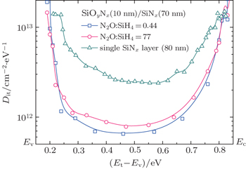
The R also affects the energy distribution of the Dit in the band gap. The variations of measured Dit with energy level in the band gap of post-RTA SiOyNx (10 nm)/SiNx (70 nm) stacks for different N2O:SiH4 ratios are shown in Fig.
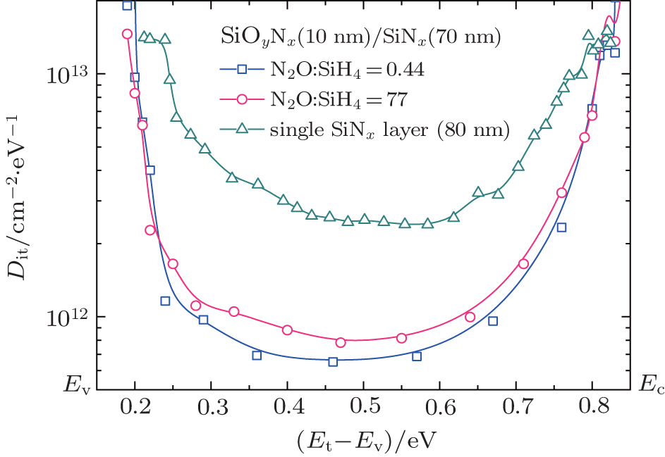 | Fig. 3. Energy distribution of Dit in the band gap for the post-RTA SiOyNx (10 nm)/SiNx (70 nm) stacks with the single SiNx (100 nm) layer as reference. The SiOyNx layers are deposited at different R values with the deposition temperature of 130 °C. |
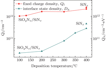
The effect of the deposition temperature on the electrical properties of the interface between the SiOyNx/SiNx stacks and the Si substrate is studied. The Dit and Qf of the stacks and the single SiNx layer-coated silicon wafers are summarized in Fig.
 | Fig. 4. Summary of the electrical parameters of the SiOyNx (30 nm)/SiNx (70 nm) stacks, including Qf and Dit, with the single SiNx (100 nm) film as reference. The SiOyNx layers are deposited at different deposition temperatures of 100 °C–400 °C, with R = 1.54. |
The Seff of the SiOyNx (30 nm)/SiNx (70 nm) stacks is obtained through the QSSPC measurement at an injection level of Δn = 7 × 1014 cm−3. The effect of the N2O/SiH4 gas flow ratio (R) is presented in Fig.
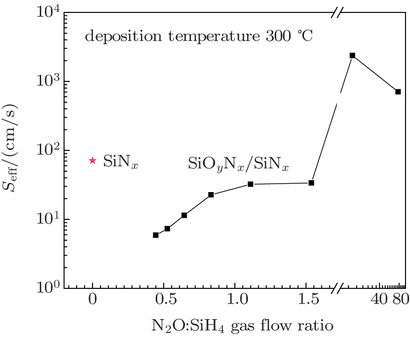 | Fig. 5. Seff of the post-RTA SiOyNx (30 nm)/SiNx (70 nm) stacks at an injection level of Δn = 7 × 1014 cm−3 through QSSPC with the single SiNx (80 nm) layer as reference. The SiOyNx layer is deposited at different R values with the deposition temperature of 300 °C. |
The effect of the deposition temperature is presented in Fig.
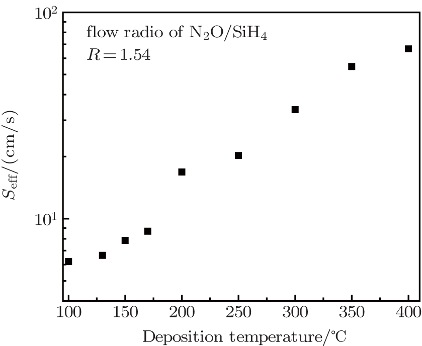 | Fig. 6. Seff of the post-RTA SiOyNx (30 nm)/SiNx (70 nm) stacks at a corona charge injection level of Δn = 7 × 1014 cm−3 through QSSPC. The SiOyNx layer is deposited at different deposition temperatures, with R = 1.54. |
Low interface state density (Dit) and fixed charge density (Qf) are obtained after a thin SiOyNx layer has been inserted between the capping SiNx layer and the silicon wafer. The small hysteresis for stack in C–V curve indicates that there exists a lower charge-trapping state density in the stack than that in the single SiNx film. Other oxygen-related defects are induced in the films by increasing the O content and minimizing H content in the SiOyNx films as R increases. The minimum value of Dit in the energy distribution of the sample with a stack rises with the increase of R by one order of magnitude lower than the one with a single SiNx layer. The Seff varies from 6 cm/s to 35 cm/s as R increases from 0.44 to 1.54. This Seff is lower than the Seff (71 cm/s) of the single SiNx layer. The minimum value of Dit of the stack in the band gap rises with the deposition temperature increasing in a range from 100 °C to 400 °C. Good passivation properties, such as Seff = 6 cm/s, are obtained at low deposition temperature. The correlation between Dit and Seff indicates that although the field-effect passivation may contribute to the passivation of the silicon surface, the chemical passivation from the stack dominates the entire passivation process.
| 1 | |
| 2 | |
| 3 | |
| 4 | |
| 5 | |
| 6 | |
| 7 | |
| 8 | |
| 9 | |
| 10 | |
| 11 | |
| 12 | |
| 13 | |
| 14 | |
| 15 | |
| 16 | |
| 17 | |
| 18 | |
| 19 | |
| 20 | |
| 21 | |
| 22 | |
| 23 | |
| 24 | |
| 25 | |
| 26 |