† Corresponding author. E-mail:
Projected supported by the National Natural Science Foundation of China (Grant Nos. 61076113 and 61274085), the Natural Science Foundation of Guangdong Province (Grant No. 2016A030313474), and the University Development Fund (Nanotechnology Research Institute, Grant No. 00600009) of the University of Hong Kong, China.
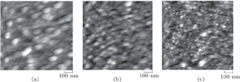
Si-doped zinc oxide (SZO) thin films are deposited by using a co-sputtering method, and used as the channel active layers of ZnO-based TFTs with single and dual active layer structures. The effects of silicon content on the optical transmittance of the SZO thin film and electrical properties of the SZO TFT are investigated. Moreover, the electrical performances and bias-stress stabilities of the single- and dual-active-layer TFTs are investigated and compared to reveal the effects of the Si doping and dual-active-layer structure. The average transmittances of all the SZO films are about 90% in the visible light region of 400 nm–800 nm, and the optical band gap of the SZO film gradually increases with increasing Si content. The Si-doping can effectively suppress the grain growth of ZnO, revealed by atomic force microscope analysis. Compared with that of the undoped ZnO TFT, the off-state current of the SZO TFT is reduced by more than two orders of magnitude and it is 1.5 × 10⁻¹² A, and thus the on/off current ratio is increased by more than two orders of magnitude. In summary, the SZO/ZnO TFT with dual-active-layer structure exhibits a high on/off current ratio of 4.0 × 10⁶ and superior stability under gate-bias and drain-bias stress.
Zinc oxide (ZnO)-based semiconductors that are used as active channel layers for thin film transistors (TFTs) have recently attracted a great deal of attention due to their advantages such as high field-effect mobilities, good uniformities, high transparencies in the visible light range, compatibility with the conventional a-Si TFT fabrication process, and low-temperature deposition process used for flexible electronics.[1–3] These excellent characteristics could meet the requirements for faster switching speed, lower power consumption and higher resolution for next-generation active-matrix liquid-crystal displays (AMLCDs) and active-matrix organic light-emitting diode (AMOLED) displays. Over the past two decades, most of the high-performance ZnO-based TFTs are based on indium-incorporated oxide semiconductors, e.g., indium zinc oxide (IZO),[4] indium zinc tin oxide (IZTO),[5] indium hafnium zinc oxide (IHZO),[6] and indium gallium zinc oxide (IGZO).[7] However, indium is relatively rare in Earth’s crust, which makes those technologies easily subject to a material shortage. Some researchers have recently reported some new oxide semiconductors free of indium, which may be used as alternative channel materials for oxide TFTs, including aluminum zinc tin oxide (AZTO),[8] zinc tin oxide (ZnSnO),[9] and silicon zinc oxide (SZO).[10] Among these elements, silicon (Si) is an abundant element in the Earth, and an appropriate Si content in ZnO-based film can not only achieve stable and dense films, but also suppress the formation of oxygen vacancies efficiently, due to its high oxygen bonding ability.[11] In addition, a dual-active-layer structure was adopted to achieve both better electrical performance and bias stability by combining two semiconducting thin film channel layers having different compositions.[12–14] In this work, active single and bilayer structure TFT with silicon-doped ZnO (SZO) thin film employed as the channel layer are fabricated by using a co-sputtering method. Effects of silicon content on optical transmittance of the SZO thin film and electrical properties of the SZO-TFT are investigated. Moreover, the electrical performances and bias stabilities of the single- and dual-active-layer TFTs are investigated and compared to reveal the effects of Si doping and dual-active-layer structure.
The schematic TFT structure is shown in Fig.
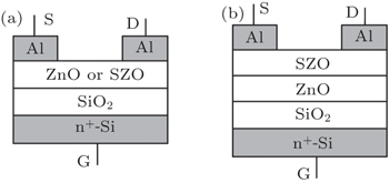 | Fig. 1. Schematic diagram of TFT devices preparing (a) ZnO or SZO thin film as a single active layer, (b) SZO/ZnO thin film as a double active layer. |
The thickness values of the silicon oxide and active layers were measured by spectroscopic reflectometer (Ocean Optics, NanoCalc-2000). The optical transmittancies of the SZO and ZnO films were measured by using a UV/visible spectroscope (Agilent, Cary 60). The values of electrical resistivity (ρ) of the films were measured by using a four-point probe resistivity measurement system (Four Probes Tech., RTS-9) and the results are shown in Table
In order to analyze the optical transmittancies of the SZO thin films with different Si content in the visible light range, the ZnO and SZO films are deposited on the top of a glass slide. Figure

 | Fig. 2. Optical transmission spectra of the SZO thin films with different Si contents. The inset shows the direct optical band gaps of the SZO films. |
Figures
Figure


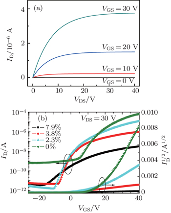 | Fig. 4. (a) Output characteristics of the SZO TFT with 2.3% Si content, (b) transfer characteristics of the SZO-TFTs with different Si content at VDS = 30 V. |
| Table 1. Main performance parameters of the SZO-TFTs with different Si content for single active layer and the SZO/ZnO TFT for double active layer. . |
In order to suppress the reductions of carrier mobility and on-state current caused by Si doping in the single-layered SZO TFT, an SZO/ZnO TFT with a double-active-layer structure as shown in Fig.
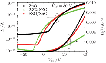 | Fig. 5. Transfer characteristics of ZnO-based TFTs with single- and dual-active-layer structures at VDS = 30 V. |
Among the three types of active layer structures, the SZO/ZnO TFT exhibits the best device performance. Compared with that of the 2.3% SZO TFT, although the off-state current of the SZO/ZnO TFT increases by one order of magnitude, the carrier mobility and on-state current both increase by one order of magnitude, and thus the on/off current ratio remains relatively high (at 4.0 × 10⁶). Compared with that of ZnO TFT, the off-state current of the SZO/ZnO TFT decreases from 0.66 nA to 13 pA, and thus the on/off current ratio increases 40 times. Moreover, there is no reduction in the carrier mobility. Therefore, the SZO/ZnO dual-active-layer structure can achieve significant improvements in low-power operation and current-drive capability. Lower off-state current in the SZO/ZnO TFT with no reduction in carrier mobility can be explained as follows. A homojunction is formed between the SZO and ZnO layers due to their different energy bandgap structures, and thus forming an energy barrier at the SZO/ZnO interface for suppressing the off-state current. In addition, since the ionic potential of Si4+ is higher than that of Zn2+,[16] silicon oxide is formed more easily than zinc oxide in the sputtering process to suppress the oxygen vacancy and charge carrier, thus resulting in less oxygen vacancy and denser structure in the SZO film than in the ZnO film. Therefore, in the SZO/ZnO structure, the top SZO film can effectively protect the bottom ZnO channel from being influenced by the oxygen and water vapor in the air.
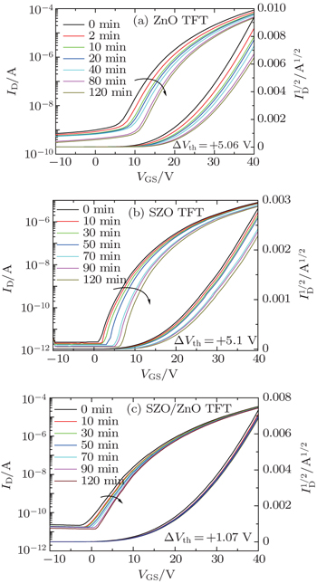
The electrical stabilities of the TFTs with single- and double-active layer structures are examined under positive gate-bias stress (PBS) and positive drain-bias stress (DBS), respectively. A gate bias VGS of 20 V is applied to the gate electrode, with the source and drain electrodes connected to the ground (0 V) during the PBS, while a drain-bias VDS of 20 V is applied to the drain electrode, with the source and gate electrodes grounded during the DBS. Figure
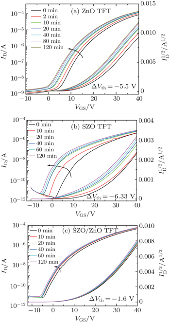
Figure
Active single- and bilayer structure thin-film transistors (TFTs) with Si-doped zinc oxide (SZO) and undoped zinc oxide (ZnO) thin film layers are fabricated by using a co-sputtering method. The doping of Si in the ZnO TFT reduces effectively the off-state current by more than two orders of magnitude and increases the on/off current ratio by more than two orders of magnitude due to the decrease of carrier concentration in the active channel layer, although the mobility is degraded. Compared with the active single-layer structure TFT with SZO and ZnO thin film, the active bilayer structure TFT with the combination of SZO and ZnO thin film layers exhibits a better electrical performance with both high on/off current ratio and high carrier mobility. On the other hand, the active bilayer structure TFT also shows a superior stability under gate- and drain-bias stresses, which is suitable for its application to AMLCD and AMOLED backplanes.
| 1 | |
| 2 | |
| 3 | |
| 4 | |
| 5 | |
| 6 | |
| 7 | |
| 8 | |
| 9 | |
| 10 | |
| 11 | |
| 12 | |
| 13 | |
| 14 | |
| 15 | |
| 16 | |
| 17 | |
| 18 | |
| 19 | |
| 20 | |
| 21 | |
| 22 | |
| 23 | |
| 24 | |
| 25 |


