Improvement in the electrical performance and bias-stress stability of dual-active-layered silicon zinc oxide/zinc oxide thin-film transistor
Liu Yu-Rong1, 2, †,  , Zhao Gao-Wei1, Lai Pai-To3, Yao Ruo-He1, 2
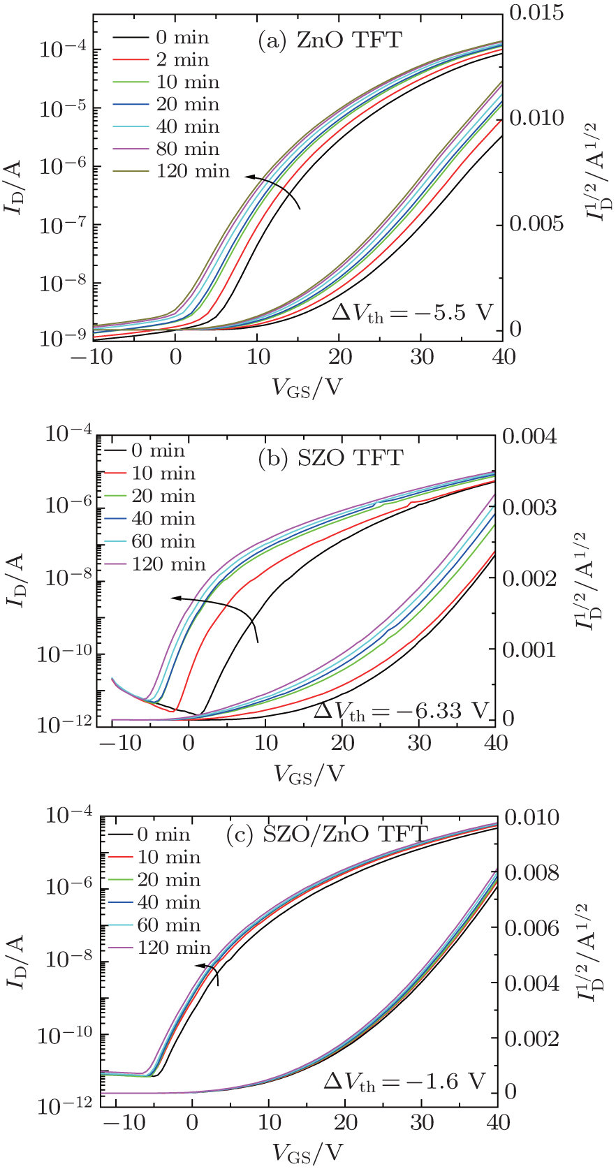
, Zhao Gao-Wei1, Lai Pai-To3, Yao Ruo-He1, 2 Transfer characteristics of the ZnO-based TFTs with single- and dual-active-layer structures at