† Corresponding author. E-mail:
Project supported by the State Key Program of the National Natural Science Foundation of China (Grant No. 61234006), the Open Foundation of the State Key Laboratory of Electronic Thin Films and Integrated Devices, China (Grant No. KFJJ201301), and the National Science and Technology Major Project of the Ministry of Science and Technology, China (Grant No. 2013ZX02305-003).
The effect of the mesa configuration on the reverse breakdown characteristic of a SiC PiN rectifier for high-voltage applications is analyzed in this study. Three geometrical parameters, i.e., mesa height, mesa angle and mesa bottom corner, are investigated by numerical simulation. The simulation results show that a deep mesa height, a small mesa angle and a smooth mesa bottom (without sub-trench) could contribute to a high breakdown voltage due to a smooth and uniform surface electric field distribution. Moreover, an optimized mesa structure without sub-trench (mesa height of 2.2 μm and mesa angle of 20°) is experimentally demonstrated. A maximum reverse blocking voltage of 4 kV and a forward voltage drop of 3.7 V at 100 A/cm2 are obtained from the fabricated diode with a 30-μm thick N− epi-layer, corresponding to 85% of the ideal parallel-plane value. The blocking characteristic as a function of the JTE dose is also discussed for the PiN rectifiers with and without interface charge.
The silicon carbide based device is a potential candidate to replace silicon in a high-performance power electronic system due to its superior properties like a wide bandgap (3.26 eV), high breakdown field (3 MV/cm), large thermal conductivity (4.9 W/cm·K) and high electron saturation velocity (2×107 cm/s).[1] For the advanced power distribution and transmission system application, the 4H–SiC PiN rectifier and IGBT transistor offer much-reduced on-state power losses compared with their unipolar counterparts, owing to the conductivity modulation effect.[2,3] In the literature, a space-modulated junction termination extension,[4] multiple-floating-zone termination extension,[5] etched JTE,[6] and mesa combined with JTEs[7–9] have been investigated for high-voltage SiC PiN devices. Among them, mesa combined with JTE structure is the most widely analyzed and manufactured. The mesa configuration plays a critical role in eliminating the electric field crowding for the SiC PiN rectifier. However, few studies of mesa shape dependence of the reverse blocking characteristic have been performed to date.
The influence of mesa architecture on the reverse blocking characteristic of a power 4H–SiC PiN rectifier is analyzed through two-dimensional (2D) Silvaco-TCAD simulations. Three geometrical parameters are considered, i.e., height, angle, and bottom corner. The improved mesa structure, formed by inductively coupled plasma (ICP), is fabricated for investigating the effect of mesa configuration on the breakdown characteristics of the rectifier. The best achieved breakdown voltage from the rectifier on the 30 μm epi-layers is 4 kV, corresponding to about 85% of the theoretical value. The dependences of JTE dose and SiO2/SiC interface charge on the reverse blocking voltage are also experimentally discussed.
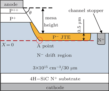
The two-dimensional numerical device characteristics are realized with Atlas from Silvaco. The details of the 4H–SiC material parameters and simulation method are presented elsewhere.[10] In addition to basic models for mobility, carrier generation-recombination, incomplete ionization of impurities and bandgap, an anisotropic impact ionization model is also developed for 4H–SiC material.[11]
Figure
The most critical aspects when designing a 4H–SiC PiN rectifier are the influences of JTE and mesa shape at the concave corner at mesa sidewall bottom on reverse breakdown voltage value. The sub-trench at the mesa bottom corner is usually observed in SiC mesa etching as shown in Fig.
Figure
 | Fig. 3. Sub-trench depth dependences of reverse blocking characteristic for 4H–SiC PiN rectifiers with and without sub-trench. |
 | Fig. 4. Simulated electric field profiles for PiN rectifiers with (a) and without (b) sub-trench at the breakdown (mesa height of 3 μm and mesa angle of 60°). |
Figure
 | Fig. 6. Surface electric field distributions through the concave corner at mesa sidewall bottom for 4H–SiC PiN rectifiers. |
Figure
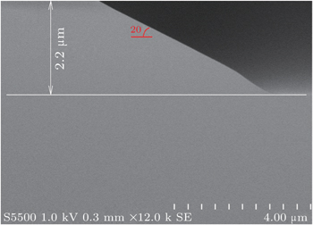
An optimized mesa configuration for the SiC PiN rectifier with a total chip area of 0.056 mm2–6.8 mm2 is experimentally investigated, and the results are shown in Fig.
Figure
 | Fig. 10. Plots of forward current density versus forward voltage of fabricated PiN rectifiers, measured at different temperatures. |
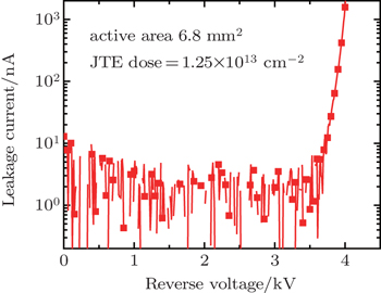
The relation between leakage current and reverse voltage is measured by using a Cascade Microtech probe and an Agilent B1505A Power Device Analyzer. The chips are immersed in fluorinert to prevent it from arcing in air condition tests. The breakdown voltage up to 4 kV of 4H–SiC PiN rectifiers with a die size of 6.8 mm2 at room temperature is shown in Fig.
 | Fig. 11. Plot of leakage current versus reverse voltage of a 4-kV PiN diode with a die size of 6.8 mm2. |
Surface passivation techniques are widely used in Si and SiC technologies to eliminate surface leakage current and enhance the breakdown of the device. However, there exists negative charge originating from electron trapping at the shallow acceptor-like interface state in SiO2/n-SiC (epilayer) or positive charge caused by holes trapped at the energetically deep interface states and the fixed oxide charge in the SiO2/p-SiC (JTE region) interface during the passivation layer formation process,[14–16] which results in a serious influence on the breakdown voltage. Because the interface charge will change by the passivation condition and may vary inside the same wafer, both positive charge and negative charge are simultaneously assumed to be in a range from 1×1012 cm−2 to 3×1012 cm−2 in our simulation. Figure
This work focuses on three geometrical parameters, i.e., mesa height, mesa angle, and mesa bottom corner for 4H–SiC PiN rectifiers. The influence of mesa configuration on the reverse blocking voltage is numerically simulated and experimentally studied. Results show that a deep mesa height, a small mesa angle and a smooth mesa bottom (without sub-trench) could contribute to a high breakdown voltage due to a smooth and uniform surface electric field distribution. By employing an optimized mesa structure, the best achieved breakdown voltage from the diodes on the 30-μm epi-layers is 4 kV, corresponding to about 85% of the theoretical value. In addition, the effect of interface charge on the breakdown voltage is also discussed.
| 1 | |
| 2 | |
| 3 | |
| 4 | |
| 5 | |
| 6 | |
| 7 | |
| 8 | |
| 9 | |
| 10 | |
| 11 | |
| 12 | |
| 13 | |
| 14 | |
| 15 | |
| 16 |


