
Low frequency noise and radiation response in the partially depleted SOI MOSFETs with ion implanted buried oxide
[Liu Yuana) , Chen Hai-Bob) , Liu Yu-Rongc) , Wang Xind) , En Yun-Feia) , Li Binc) , Lu Yu-Dong†a)  ]
]
]
|
|


†Corresponding author. E-mail: luyd@ceprei.com
*Project supported by the National Natural Science Foundation of China (Grant Nos. 61204112 and 61204116).
Low frequency noise behaviors of partially depleted silicon-on-insulator (PDSOI) n-channel metal-oxide semiconductors (MOS) transistors with and without ion implantation into the buried oxide are investigated in this paper. Owing to ion implantation-induced electron traps in the buried oxide and back interface states, back gate threshold voltage increases from 44.48 V to 51.47 V and sub-threshold swing increases from 2.47 V/dec to 3.37 V/dec, while electron field effect mobility decreases from 475.44 cm2/V·s to 363.65 cm2/V·s. In addition, the magnitude of normalized low frequency noise also greatly increases, which indicates that the intrinsic electronic performances are degenerated after ion implantation processing. According to carrier number fluctuation theory, the extracted flat-band voltage noise power spectral densities in the PDSOI devices with and without ion implantation are equal to 7×10⁻¹⁰ V2·Hz−1 and 2.7×10⁻⁸ V2·Hz−1, respectively, while the extracted average trap density in the buried oxide increases from 1.42×1017 cm−3·eV−1 to 6.16×1018 cm−3·eV−1. Based on carrier mobility fluctuation theory, the extracted average Hooge’s parameter in these devices increases from 3.92×10⁻⁵ to 1.34×10⁻² after ion implantation processing. Finally, radiation responses in the PDSOI devices are investigated. Owing to radiation-induced positive buried oxide trapped charges, back gate threshold voltage decreases with the increase of the total dose. After radiation reaches up to a total dose of 1 M·rad(si), the shifts of back gate threshold voltage in the SOI devices with and without ion implantation are −10.82 V and −31.84 V, respectively. The low frequency noise behaviors in these devices before and after radiation are also compared and discussed.
Silicon-on-insulator (SOI) technology has been widely used in space applications and offers some advantages in hardness over bulk silicon or epitaxial silicon technologies, such as reduced transient radiation response and freedom from latch-up effect.[1] However, when they are exposed to ionizing radiation, the buried oxide becomes positively charged by the radiation-induced trapping holes.[2] The resulting shift in the back gate threshold voltage may adversely affect device operation and circuit performance.[3, 4]
It has been reported that high fluence ion implantation (such as Al, Si, P or Ge) into the buried oxide can be used to reduce the shift in back gate threshold voltage during exposure to ionizing radiation by creating electron traps with a very large capture cross section and compensating for trapped positive charges when being filled with electrons.[4– 10] For example, Mrstik et al.[6] studied charge trapping in thermal oxides implanted with up to 5× 1015 cm− 2 of Al, Si, P. They found that the capture cross section (1× 10− 13 cm2 is large in electron trap formed at the highest implant doses, while the shift of flat-band voltage following hole injection decreases, which indicates a reduction of hole trapping near the Si– SiO2 interface. However, near interface shallow electron traps are created by ion implantation, which leads to large bias instability at the interface between silicon and buried oxide.[11, 12] Hence, the intrinsic electrical performance at the Si– SiO2 interface may degenerate. There may be some room to study the effects of ion implantation and, therefore, metastable electron traps in the buried oxide on the SOI device properties.
Low frequency noise measurements can be used as a valuable diagnostic tool for quality and reliability evaluations of semiconductor devices.[12– 16] Deep traps in the gate oxide and buried oxide of SOI metal-oxide semiconductor field effect transistors (MOSFETs), which are situated close to the quasi-Fermi level energy, can be probed by low frequency noise measurements. Low frequency noise can also be used to characterize surface states and border traps in the SOI MOSFETs.[17] A low frequency noise measurement can be valuable for an accurate treatment of intrinsic electrical performance and influence of defects in the buried oxide because it partly reveals the internal physics of the device examined.
In this paper, the low frequency noises and radiation responses in the partially depleted (PD) SOI n-channel metal– oxide semiconductor (NMOS) transistors with and without ion implantation are comparatively studied. From low frequency noise measurements, the flat-band spectral densities are extracted and then the concentrations of defects near Si– SiO2 interface are calculated. According to carrier number fluctuation theory, the spatial distribution of trapped charges in the buried oxide is extracted. By considering the carrier mobility fluctuation theory, the average Hooge’ s parameters are extracted and then the intrinsic electrical performances in these SOI devices are compared. Finally, the variations of back gate threshold voltage and low frequency noise with total ionizing dose are discussed.
PDSOI NMOS transistors were processed by using a 0.8-μ m complementary-MOS (CMOS) SOI technology with four types of buried oxide processings for the starting wafers (named wafers A– D). Wafer A did not receive any ion implantation during processing, while wafers B– D received special process treatments to introduce electron traps into the buried oxide layer. Wafers B– D were implanted with ions with similar high fluence levels prior to transistor fabrication. Therefore, the implant conditions used for wafer D were expected to result in more electron traps than that for wafer C, while wafer B had the lowest concentration of electron traps in these devices.
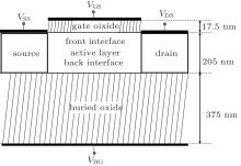
Figure 1 shows the cross section view of PDSOI device. The thickness of silicon film (tsi) is about 205 nm, while the thickness of gate oxide (tox) is about 17.5 nm, and the thickness of buried oxide (tbox) is 375 nm. The calculated gate oxide capacitance per unit area (Cox) is about 1.97× 10− 7 F/cm2, and the calculated buried oxide capacitance per unit area (Cbox) is about 9.2× 10− 9 F/cm2. The channel length (L) is 8 μ m, and the channel width (W) is 8 μ m.
 | Fig. 1. Cross section view of PDSOI device. |
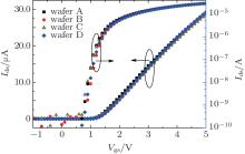
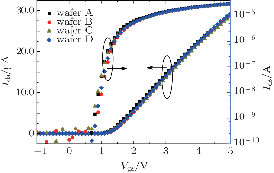
The front gate and back gate transfer characteristics of PD SOI devices from wafer A to wafer D are shown in Figs. 1 and 2.
As shown in Fig. 2, the front gate transfer characteristics are similar in these devices. In the device from wafer A, the front gate threshold voltage is about 1.23 V, the electron field effect mobility in the Si– SiO2 interface between gate oxide and active layer (defined as front interface) is about 391.2 cm2/V · s, and the front gate sub-threshold swing is about 0.16 V/dec.
 | Fig. 2. Front gate transfer characteristics in the PDSOI devices with four types of buried oxides. |
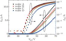
As shown in Fig. 3, positive shifts of back gate transfer characteristics are observed with the increase of electron trap concentration. The back gate threshold voltages in the devices from wafer A to wafer D are about 44.48 V, 46.37 V, 48.05 V, and 51.47 V, respectively. The values of electron field effect mobility in the Si– SiO2 interface between buried oxide and active layer (defined as back interface) are 475.44 cm2/V · s, 449.5 cm2/V · s, 445.16 cm2/V · s, and 363.65 cm2/V · s, respectively. The back gate sub-threshold swings are about 2.47 V/dec, 2.98 V/dec, 2.85 V/dec, and 3.37 V/dec, respectively. As the ion implantation fluence level increases, the intrinsic electrical performances in the back interface become degenerated.
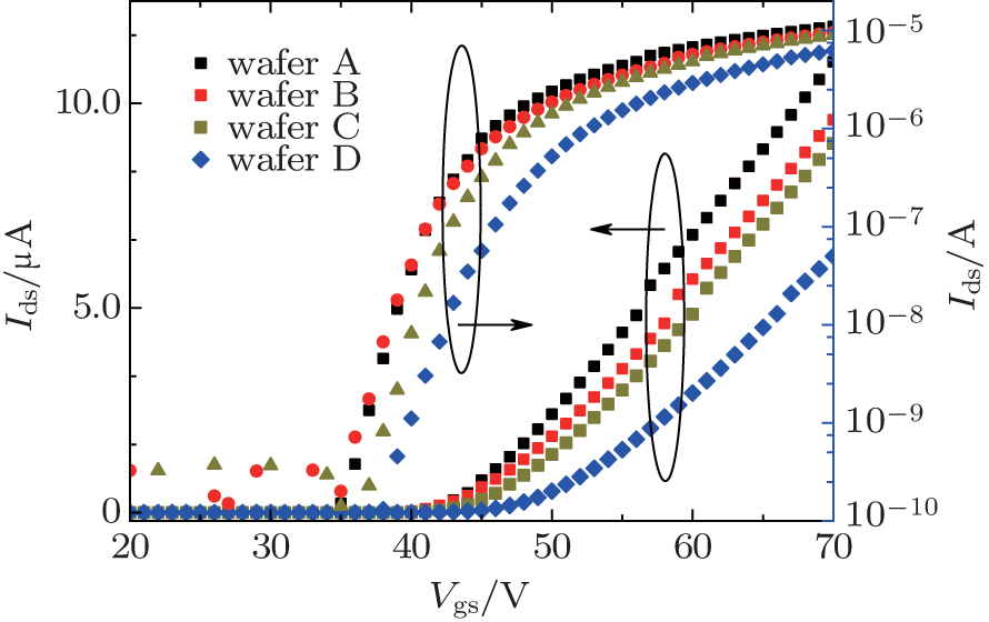 | Fig. 3. Back gate transfer characteristics in the PD-SOI devices with four types of buried oxides. |
The shift of back gate sub-threshold swing (Δ S) in each of these devices can be directly converted into the interface state density (Δ Dit) located near buried oxide which is created by ion implantation, and expressed as[14]

where k is the Boltzmann’ s constant, T is the temperature, the extracted values of Δ Dit are about 4.9× 1011 cm− 2· eV− 1, 3.65× 1011 cm− 2· eV− 1, and 8.65× 1011 cm− 2· eV− 1 for wafers B, C, and D, respectively. The bulk potential φ n for n-channel SOI NMOS transistor is about 0.38 eV. Thus, the calculated densities of ion implantation-induced interface state Δ Nit are about 1.86× 1011 cm− 2, 1.39× 1011 cm− 2, and 3.29× 1011 cm− 2 for wafers B, C, and D, respectively.[16] Therefore, more interface traps are observed in the SOI devices with high fluence level of ion implantation. Moreover, positive shifts of back gate threshold voltage and flat-band voltage are also partly caused by the interface traps which are created during the ion implantation process.
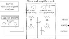
The electrical properties of SOI NMOS transistors were measured by a PC controlled Agilent B1500 semiconductor parametric analyzer. The experiment setups to measure the SOI NMOS transistor drain current noise power spectrum under different bias conditions are illustrated in Fig. 4.[18] The device under test (DUT) is voltage-biased, and its current noises are analyzed by using of SR785 dynamic signal analyzer. The core of this system is the filter and amplifier unit which is also named as 9812B noise analyzer made by Proplus Design Solution, Inc. The unit contains a high quality RC low-pass filter that is used to remove the source-measure unit noise from B1500. Thus, the DUT bias voltages are very close to the pure DC signals and free from noise. In the whole measurements, the selected Rg was shorted (0 Ω ) due to the high gate impedance and the selected Rd value was 33 or 100 k· Ω .
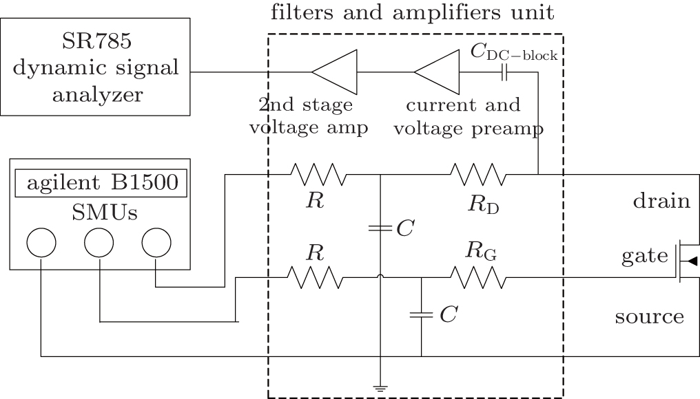 | Fig. 4. Measurement setup for low frequency noise in the SOI NMOS transistor.[17] |
The radiation experiments were performed by using Co60 source with a dose rate of 87.85 rad(si)/s. According to the worst case of bias condition proposed by Refs. [19]– [20], the devices were irradiated with transfer gate (TG) bias. In the TG bias, gate & body and back gate were connected to the ground while drain and source were connected to VDD.
The transfer characteristics in the PDSOI devices were measured at 20 min after ionizing irradiation, while the low frequency noises were measured at 1.5 h after ionizing irradiation.
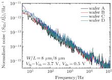
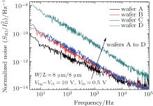
Low frequency noises are measured under front gate and back gate operations in the SOI NMOS transistors with four types of buried oxides. The measured results of low frequency noise in the front gate at Vfg– Vth = 3.7 V and Vds = 0.5 V for these devices are shown in Fig. 5, while the results of low frequency noise in the back gate at Vbg– Vth = 10 V and Vds = 0.5 V are shown in Fig. 6.
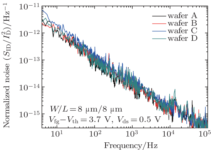 | Fig. 5. Measured low frequency noises under front gate operation in the PD SOI devices with four types of buried oxides at Vfg– Vth = 3.7 V and Vds = 0.5 V. |
It is obvious that the low frequency noises under front gate and back gate operations follow the 1/f behavior in these devices. According to carrier number fluctuation (Δ n) theory, the 1/f waveform is a superposition of a large number of relaxation processes with a wide spread of time constants.[18] The relaxation process can originate from the electron random trapping/detrapping and the distribution of trapping times might arise from the tunneling of charge from the semiconductor surface to traps located in the oxide.[21] Based on McWhorter’ s model, the normalized drain current noise power spectral density 
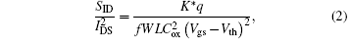
where K* is a coefficient relating to the tunneling possibility between channel and gate insulator traps, and increases with increasing oxide trap density and interface trap density, f is the frequency, and Vgs– Vth is the overdrive voltage.
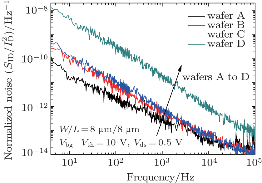 | Fig. 6. Measured low frequency noises under back gate operation in the PDSOI devices with four types of buried oxides at Vbg– Vth = 10 V and Vds = 0.5 V. |
As shown in Fig. 5, the front gate normalized drain current noise power spectral densities are quite similar in the devices with and without ion implantation into buried oxide. This indicates that gate oxide and front interface may be less affected by ion implantation, which validates the above DC analysis results under front gate operation of PDSOI devices.
As shown in Fig. 6, the back gate normalized drain current noise power spectral density increases with the increase of ion implantation dose. This indicates that densities of back interface trap and electron trap located in the buried oxide may increase after ion implantation process.[11, 13]
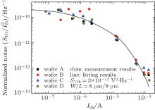
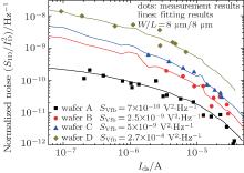
To further investigate low frequency noises in these SOI devices, the normalized channel current noise power spectra versus channel current are shown in Figs. 7 and 8.
 | Fig. 7. Plots of normalized noise versus channel current under front gate operation in the PDSOI devices with four types of buried oxides. |
Following the conventional tunneling theory, the relationship between the normalized drain current noise power spectral density and the flat-band voltage noise power spectral density (svfb) is given by[23]
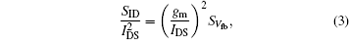
where gm is the device transconductance. By considering the uniformly distributed traps in the oxide, Svfb can be calculated by[14, 23]

where Nt is the trap state density in the oxide (cm− 3· eV− 1), and λ is the tunnel attenuation distance (about 0.1 nm in the SiO2).
Based on Eq. (3), Svfb under front gate operation can be extracted from Fig. 7 and it is about 3× 10− 12 V2· Hz− 1. Therefore, the estimation of average trap density in the gate oxide is deduced from Eq. (4) and gives Nt = 2.79× 1017 cm− 3· eV− 1.
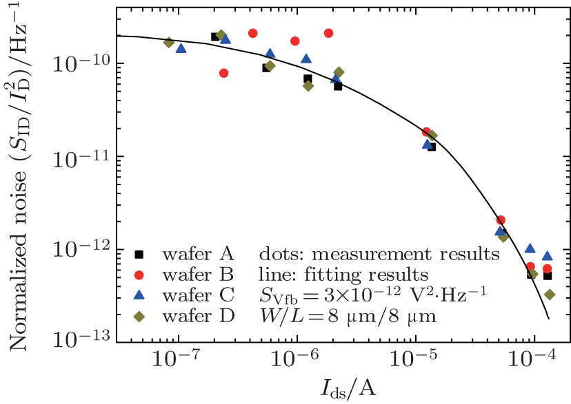
Based on Eq. (3), the values of Svfb under back gate operation can be extracted from Fig. 8, and they are about 7× 10− 10 V2· Hz− 1 for wafer A, 2.5× 10− 9 V2· Hz− 1 for wafer B, 5× 10− 9 V2· Hz− 1 for wafer C and 2.7× 10− 8 V2· Hz− 1 for wafer D. Therefore, the average trap densities in the buried oxide are deduced from Eq. (4) and they are Nt = 1.42× 1017 cm− 3· eV− 1 for wafer A, Nt = 5.07× 1017 cm− 3· eV− 1 for wafer B, Nt = 1.14× 1018 cm− 3· eV− 1 for wafer C, and Nt = 6.16× 1018 cm− 3· eV− 1 for wafer D.
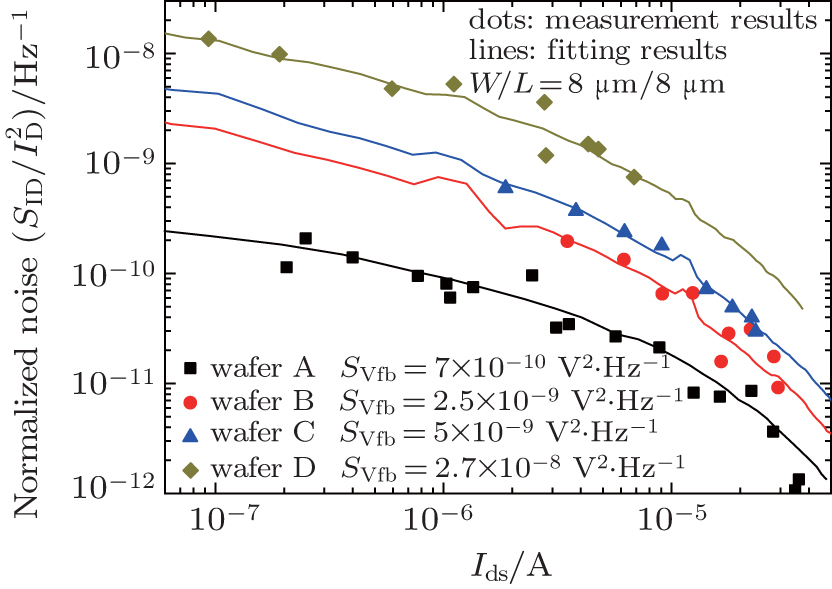 | Fig. 8. Plots of normalized noise versus channel current under back gate operation in the PDSOI devices with four types of buried oxides. |
Trapping and de-trapping of carriers tunneling from the inversion layer to the dielectric traps near the interface cause 1/f noise, with each tunneling depth corresponding to a specific time constant τ = 1/2π f . In order to have a qualitative spatial distribution of traps in the buried oxide, the frequency is converted into the tunneling depth as follows:[16, 23, 24]

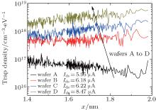
where τ 0 is the time constant at the interface, x is the distance from the back interface to the buried oxide, α t is the tunneling attenuation coefficient of the electron wave function in the gate dielectric, which for SiO2 is taken to be 108 cm− 1. The value of τ 0 is typically taken to be equal to 10− 10 s for traps distributed up to 5 nm. Equation (5) states that the probability of penetration into the buried oxide decreases exponentially with distance. The extracted trap density profiles for these SOI devices with and without ion implantation are shown in Fig. 9. The results show that trap density increases with an increase of the ion implantation dose. The extracted trap density of wafer A is a factor of about 50 smaller than that of wafer D.
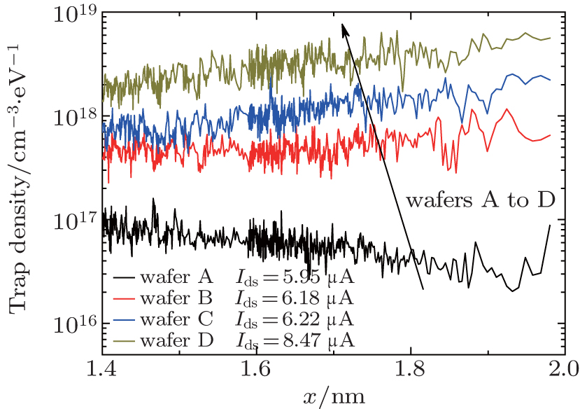 | Fig. 9. Extracted spatial distributions of trapped charges in the buried oxide of PDSOI devices. |
Hooge claimed the 1/f noise may originate from noise in lattice scattering, which in turn causes random mobility fluctuation. This result is different from McWhorter’ s carrier number fluctuation theory. According to Hooge’ s empirical law, the normalized drain current noise power spectral density 

where α H is an empirical dimensionless constant which is also called Hooge’ s parameter, and α H is technology/material dependent and could be considered as a device/material quality indicator.
The Hooge’ s parameter α H is frequently used as a figure of merit for the comparison between different device technologies and it is usually low for a higher electronic quality material.[17, 25, 26] As reported by Refs. [25] and [26], the modern IC-graded resistor has the lowest reported α H (∼ 10− 6). Depending more on sample quality and preparation condition, the values of α H for bulk silicon MOSFETs and resistors can have a widely distribution and can reach as high as 4× 10− 4. In addition, α H is about 3× 10− 3 for a-Si:H thin film transistors, [27] 10− 2 for organic thin film transistors[28] and 10− 3 for indium zinc oxide thin film transistors.[18]
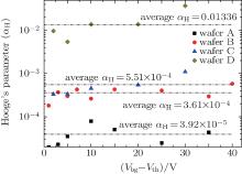
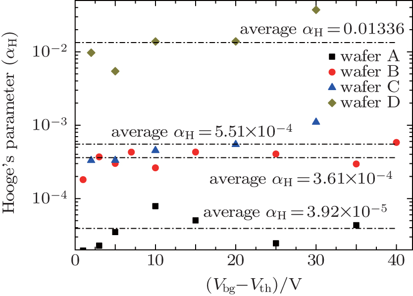
The extracted values of α H in the PD-SOI NMOS transistors with and without ion implantation are shown in Fig. 10. The results show that the extracted α H of wafer D is a factor of about 340 larger than that of wafer A. The calculated results show that intrinsic electrical performances of SOI devices with ion implantation are worse than those of SOI devices without ion implantation.
 | Fig. 10. Plots of extracted Hooge’ s parameter (α H) versus overdrive voltage (Vbg− Vth) in the back gate of SOI devices. |
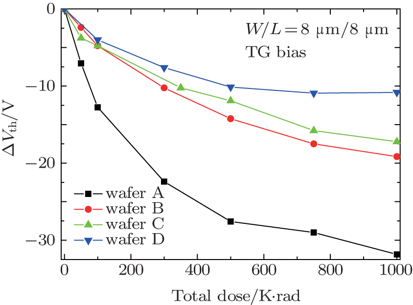
The shifts of back gate threshold voltage each as a function of total irradiation dose for SOI devices with and without ion implantation are shown in Fig. 11. During the measurements of back gate transfer characteristics, the front gate is grounded. The back gate threshold voltage shifts of four devices from wafers A, B, C, and D after 1 M· rad(si) irradiation are − 31.84 V, − 19.15 V, − 17.21 V, and − 10.82 V, respectively. The devices fabricated with ion implantation show relatively small shifts in the back gate threshold voltage, which confirms the expected reduction in the radiation-induced net positive buried oxide trapped charges.[6, 11]
 | Fig. 11. Shifts of back gate threshold voltage in the SOI devices with and without ion implantation. |
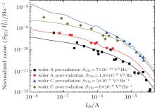
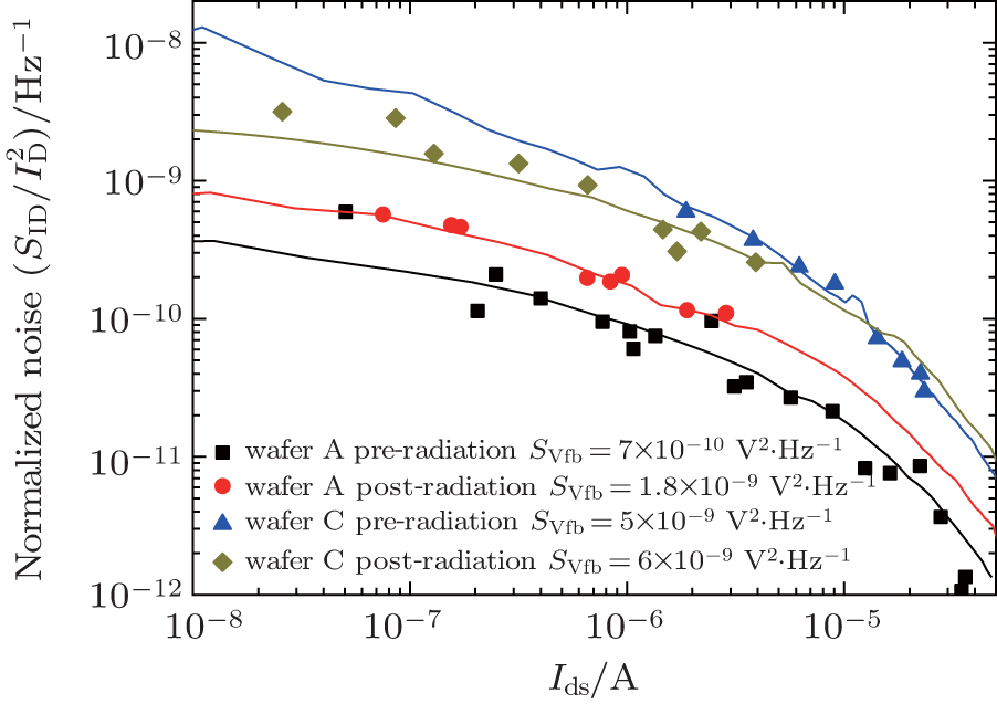
As shown in Fig. 12, the device from wafer A without ion implantation has the lowest noise before irradiation, while its noise increases most after irradiation. The device from wafer C with ion implantation has a higher noise magnitude than that from wafer A, but its noise level shows little change after irradiation with a total dose up to 1 M· rad(si). Hence, the magnitude of low frequency noise cannot be used as a prediction tool for back gate threshold voltage shift in these SOI devices, which is different from the MOSFET proposed by Fleetwood et al.[29] This is probably due to the high defect density caused by ion implantation, which makes the noise less sensitive to the radiation-induced trapped charges.[11]
 | Fig. 12. Plots of normalized noise versus channel current under back gate operation in the SOI devices before and after radiation up to 1 M rad(Si). |
As the ion implantation dose in the buried oxide of SOI transistor increases, the back gate threshold voltage and sub-threshold swing increase while the electron field effect mobility decreases. In addition, after ion implantation, the magnitude of normalized low frequency noise increases about 50 times. Meanwhile, the radiation responses in the SOI transistors are also studied. Ion implantation in the buried oxide decreases the net oxide trapped charges created during irradiation. Radiation-induced shifts of back gate threshold voltage in the devices with and without ion implantation are about − 10.82 V and − 31.84 V, while low frequency noises are not significantly varied after irradiation in the SOI devices with ion implantation. The experimental results illustrate that the ion implantation of the buried oxide can improve the total dose radiation response of SOI device by generating electron traps deep within the buried oxide, while the intrinsic electrical performances in the back interface of SOI transistors are degenerated after ion implantation.
| 1 |
|
| 2 |
|
| 3 |
|
| 4 |
|
| 5 |
|
| 6 |
|
| 7 |
|
| 8 |
|
| 9 |
|
| 10 |
|
| 11 |
|
| 12 |
|
| 13 |
|
| 14 |
|
| 15 |
|
| 16 |
|
| 17 |
|
| 18 |
|
| 19 |
|
| 20 |
|
| 21 |
|
| 22 |
|
| 23 |
|
| 24 |
|
| 25 |
|
| 26 |
|
| 27 |
|
| 28 |
|
| 29 |
|