
Plasma induced by pulsed laser and fabrication of silicon nanostructures
[Hang Wei-Qi†a)  , Dong Tai-Ge
b) , Wang Gangb) , Liu Liu Shi-Rongb) , Huang Zhong-Meia) , Miao Xin-Jiana) , Lv Quanc) , Qin Chao-Jianb) ]
, Dong Tai-Ge|
|

 , Dong Tai-Ge
†Corresponding author. E-mail: sci.wqhuang@gzu.edu.cn
*Project supported by the National Natural Science Foundation of China (Grant Nos. 11264007 and 61465003).
It is interesting that in preparing process of nanosilicon by pulsed laser, the periodic diffraction pattern from plasmonic lattice structure in the Purcell cavity due to interaction between plasmons and photons is observed. This kind of plasmonic lattice structure confined in the cavity may be similar to the Wigner crystal structure. Emission manipulation on Si nanostructures fabricated by the plasmonic wave induced from pulsed laser is studied by using photoluminescence spectroscopy. The electronic localized states and surface bonding are characterized by several emission bands peaked near 600 nm and 700 nm on samples prepared in oxygen or nitrogen environment. The electroluminescence wavelength is measured in the telecom window on silicon film coated by ytterbium. The enhanced emission originates from surface localized states in band gap due to broken symmetry from some bonds on surface bulges produced by plasmonic wave in the cavity.
The biggest challenge is to develop an efficient silicon-based light-emitting device because of the extremely low emission efficiency of silicon with an indirect band gap. During the past two decades, the photoluminescence (PL) of nanosilicon has been discussed intensively.[1– 3] Although light emission relative to quantum confinement (QC) effect of nanosilicon has been demonstrated, the QC effect is disturbed by surface states effects on a smaller nanoscale (< 3 nm) and disappears on a larger nanoscale (> 10 nm).[4– 8] There are difficulties in integrating quantum structures in a narrower nanoscale range with conventional optoelectronics.[9, 10] It is desirable to develop new concepts to obtain emission from silicon in a larger nanoscale range compatible with optoelectronics devices. Besides QC effect, many different strategies have been explored to make an efficient emitter on silicon at various strategic wavelengths, including defect emission due to doping with impurity atoms on nanosilicon surface and optically active structural defects.[11– 15]
Although very promising, the sub-band gap luminescence based on silicon is still impractical because emission intensity is strongly quenched and becomes almost undetectable at room temperature. It is good way to resolve the problem that the localized states produced from some bonds on curved surface of nanosilicon provide stable emission centers and increase the efficiency of active centers.[16, 17] In the present article, it is reported that the period diffraction pattern from plasmonic lattice structure in the Purcell cavity due to interaction between plasmon and photon has been observed in preparing process of nanosilicon by pulsed laser. The plasmonic lattice structure may be similar to the Wigner crystal structure.[18] The plasmonic wave induced by pulsed laser in the Purcell cavity could be used to prepare various nanostructures on silicon in different environments. By using different physical processes in preparation, the emission wavelength could be adjusted to visible light in oxygen or nitrogen atmosphere and to telecom window by depositing ytterbium. Here, we demonstrate that the visible light with high external quantum yield in Purcell cavity at room temperature originates from the localized state emission (different from QC effect emission) on nanosilicon prepared in an oxygen or nitrogen environment, and the optical gain in PL emission is observed at 604 nm after annealing. The PL emission and enhanced room-temperature electroluminescence (EL) in the telecom window are measured on silicon film coated by ytterbium.
It is very interesting to observe and analyze the physical process for preparing nanostructures on silicon. We use pulsed Nd:YAG laser (wavelength: 1064 nm, pulse width (FWHM): 20 ns, repetition rate: 1 kHz– 4 kHz) for preparing nanosilicon. The vibration (ω 2 = Ne2/mɛ , [19] where N is electronic density and ɛ is dielectric function) of plasma is induced by ns-pulsed laser, [2, 3] which forms a resonant standing wave in the Purcell cavity where the plasmonic wave is built 
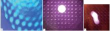
By the reflection Talbot amplifying, figure 1(a) shows the periodic pattern produced by interaction between plasmon and photon in the cavity prepared by the beam of the third harmonic of a ns-pulsed Nd:YAG laser (355 nm). The blue light image of the plasmonic standing wave with the resonant modes in the cavity is observed by eyes directly on the screen. It is the plasmonic standing wave induced by pulsed laser that could be used to prepare micro-nanostructures on silicon. The infrared image of the diffraction pattern on the plasmonic lattice structure induced by pulsed laser at 1064 nm in the cavity is shown in Fig. 1(b). As shown in Fig. 1(c), the photon trajectory of the coherent standing wave recorded by an infrared camera describes the physical process of the coupling between plasmon and photon.
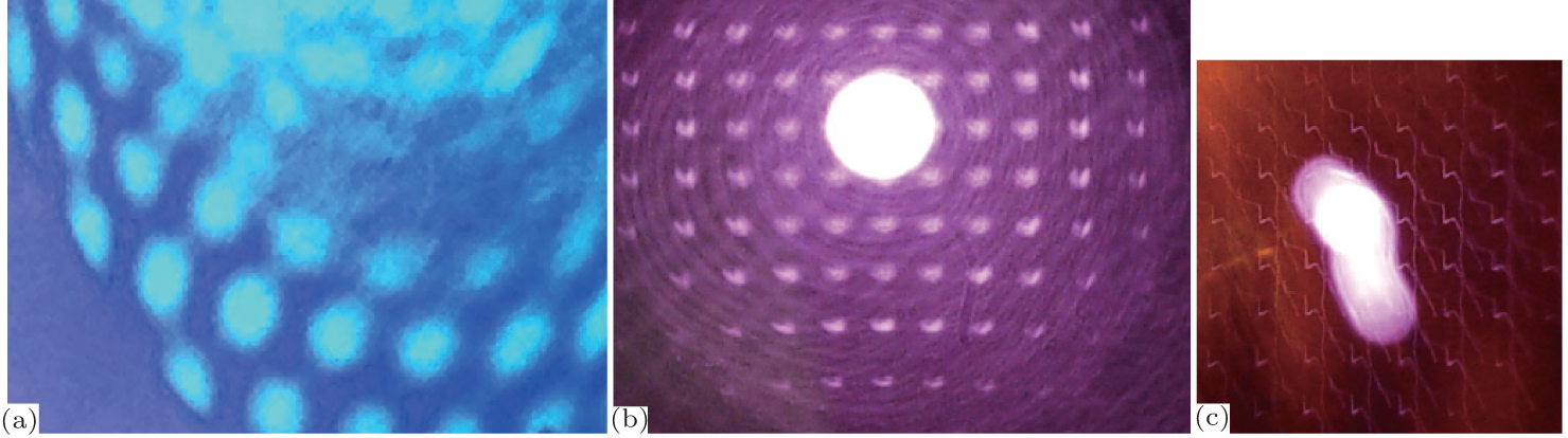 | Fig. 1. (a) Blue light image of the plasmonic standing wave produced by ns-pulsed laser at 355 nm in the cavity. (b) Plasma plume (visible light spot) and infrared image of the diffraction pattern on plasmonic lattice structures induced by pulsed laser at 1064 nm in the cavity. (c) Infrared image of photon trajectory in plasmonic emission on plasmonic lattice structures induced by pulsed laser at 1064 nm in the cavity. |
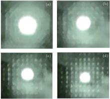
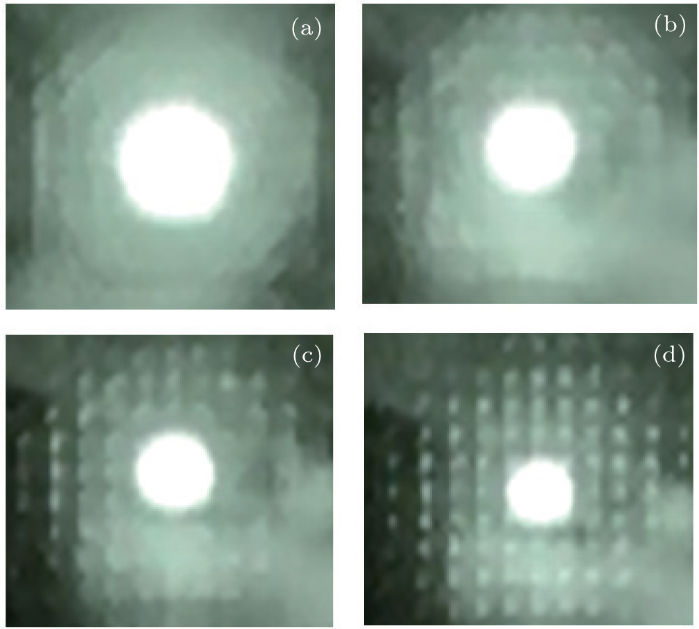 | Fig. 2. Diffraction patterns on plasmonic lattice structure under pulsed laser with different repetition rates at (a) 1 kHz, (b) 2 kHz, (c) 3 kHz, and (d) 4 kHz. |
Through increasing repetition rate of laser pulses or enlarging distance of measurement, the interference in interaction between plasmon and relaxation pulse could be built up, in which the interference photonic wave could form the plasmonic standing wave to build the plasmonic lattice structure in the cavity. It is very interesting that the diffraction pattern of the plasmonic lattice structure induced by nanosecond laser pulses is observed in the Purcell cavity of silicon. Figure 2 shows the forming process of the diffraction pattern of the plasmonic lattice structures induced by pulsed laser at 355 nm at different repetition rates of pulses, respectively at 1, 2, 3, and 4 kHz related to Figs. 2(a)– 2(d). The periodic pattern of the plasmonic lattice structure is built up because enlarging of the relaxation time of laser pulses in the cavity forms the plasmonic standing wave when the repeat rate of laser pulses reaches 4 kHz as shown in Fig. 2(d).
It is found that the spatial frequency 1/d of the plasmonic period structures ranges from 1/100 nm to 1/20 μ m due to the quantized cavity modes in the plasmonic standing wave induced by laser pulses in the cavity, in which increasing repetition rates could obtain the higher spatial frequency. It is useful to control the process of preparing micro-nanostructures on silicon. The plasmonic lattice structure due to interaction between photon and plasmon may be similar to the Wigner crystal structure.[18]
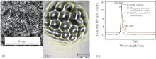
The transmission electron microscope (TEM) image in Fig. 3(a) shows the oxidized nanosilicon structures prepared by ns-pulse laser in oxygen atmosphere, and figure 3(b) shows that the micro-nanostructures on silicon remain in the cavity after preparation, in which an optical image shows the hole-net structure on a micro-scale prepared by ns-pulse laser in the cavity.
In the Raman spectrum (curve C) of Fig. 3(c), the nanosilicon size could be indicated to be several nanometers by calculating and measuring the deviation of the Raman peak (at 520.7 cm− 1 or 528.6 nm under excitation at 514 nm on bulk silicon) due to the confinement of phonons in nanoparticles on the sample. The distribution center of nanosilicon sizes is about 3 nm, and there is no stress factor to disturb the Raman measurement. It is essentially coincident with the result obtained by TEM analysis which shows that the range of the nanostructure size is about 1.7 nm– 4 nm.
 | Fig. 3. (a) TEM image of Si nanostructure oxidized. (b) Optical image of hole-net structure prepared by the plasmonic standing wave induced by ns-pulsed laser at 355 nm in the cavity, in which the inset shows qunatum dot on nanosilicon in net-hole structure. (c) Raman scattering spectra, in which the curve B is the standard Raman spectrum on bulk silicon, and the curve C relates to the Si nanostructure. |
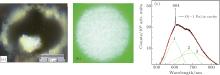
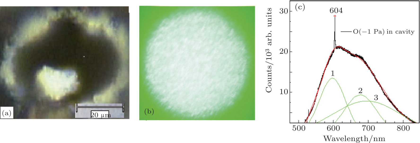 | Fig. 4. (a) Optical image of the plasmonic emission on the oxidized Si nanostructures excited by a xenon lamp in the cavity. (b) Optical image of the plasmonic emission on the oxidized Si nanostructures under the 514-nm excitation of an argon ion laser in the cavity. (c) PL spectrum on the sample (Fig. 3(a)) after annealing treatment, in which there is a sharp peak at 604 nm (optical gain coefficient > 80). |
The bright visible light emission is observed in Purcell cavity at room temperature on the nanosilicon sample prepared by ns-pulsed laser (1064 nm) in oxygen environment at a pressure of 10− 1 Pa in the chamber of the fabrication device. The optical image of the PL emission excited by a xenon lamp is shown in Fig. 4(a), the optical image of the plasmonic emission under the 514-nm excitation of argon ion laser is shown in Fig. 4(b), and the PL spectrum on the sample after annealing treatment at 1050 ° C for 20 min in nitrogen atmosphere is shown in Fig. 4(c), in which there is a sharp peak at 604 nm (optical gain coefficient > 80).
The PL is characterized in several emission bands, especially two bands peaked near 600 nm and 700 nm on nanosilicon samples prepared in an oxygen environment. The experimental results demonstrate that the emission band peaked near 600 nm (Fig. 5(a)) is stronger at smaller oxygen pressure (< 10− 1 Pa), and the emission band peaked near 700 nm (Fig. 5(b)) is enhanced at larger oxygen pressure (> 100 Pa) in the chamber of the fabrication device. The calculation results indicate that it is easier to build Si– O– Si bonds on a nanosilicon surface in diluted density of oxygen, and the energy levels of their localized states are higher than those of Si= O bonds in gap. Therefore, it is inferred that the emission peak near 600 nm (the fit peak 1 in each of Figs. 4(c), 5(a), and 5(c)) may be related to Si– O– Si bonds, and the peak near 700 nm (the fit peak 2 in each of Figs. 4(c) and 5(b)) may be due to Si= O bonds on silicon surface.
In Fig. 4(c), Fig. 5(a), and Fig.5(c), the band of the fit peak 3 is broader (from 550 nm to 830 nm), related to the range of the nanoparticles size (about 1.7 nm∼ 4 nm), in which the QC effect plays a main role.[20] The peak 3 is very good for Gaussian fit because of its random process in distribution of the nanoparticles size, and its intensity is weaker due to the spontaneous emission.[21] But the peak 1 and peak 2 are suitable for Lorenz fit due to their localized states emission. The localized states originating from surface bonds on curved nanosilicon could build the four-level system to make activation on Si nanostructure for emission.
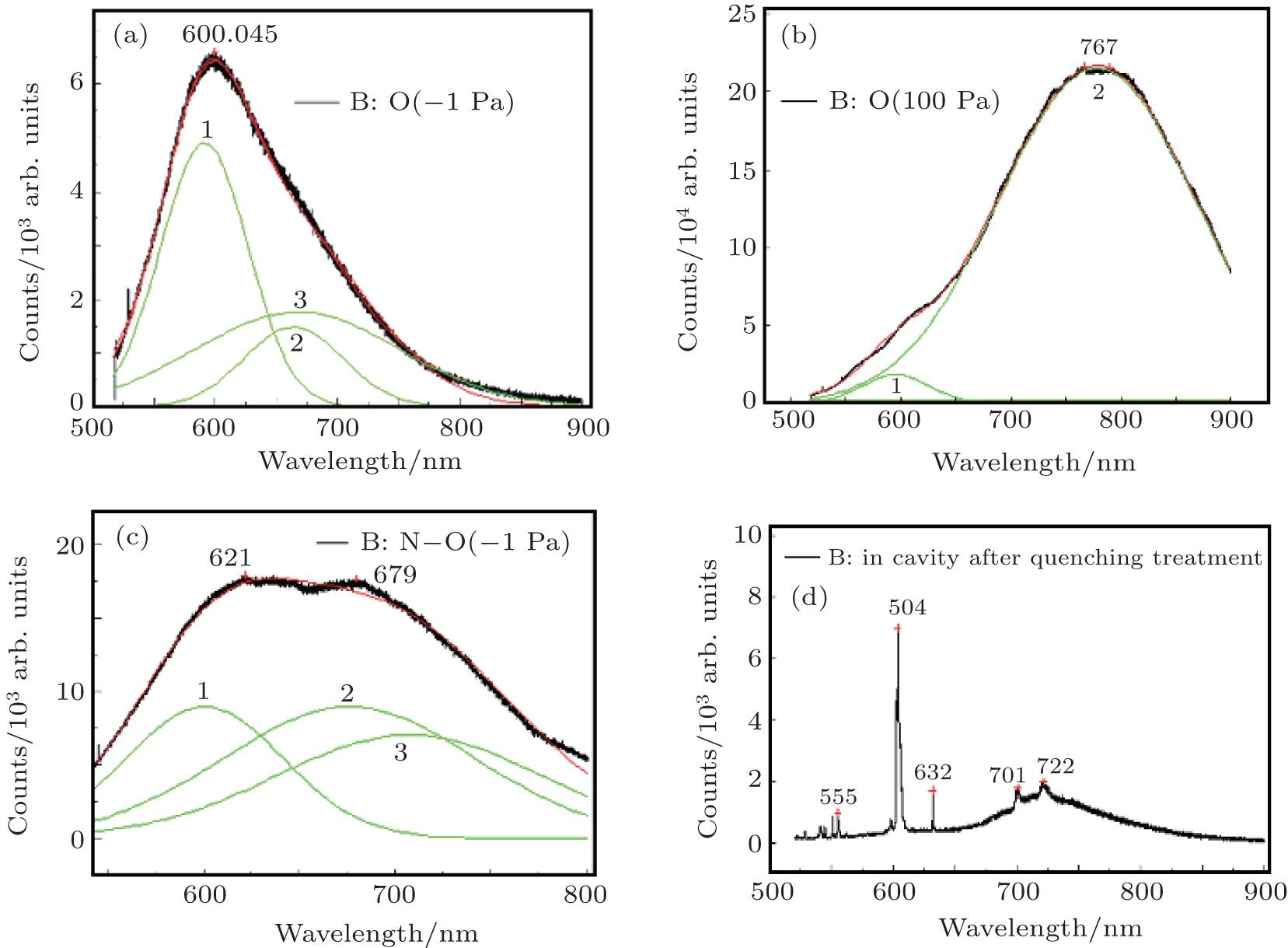 | Fig. 5. (a) PL spectrum on nanosilicon sample prepared at a smaller oxygen pressure (< 10− 1 Pa), in which the stronger fit peak 1 from Si– O– Si bonds relates to the localized states emission, the broader fit peak 3 relates to the QC effect emission. (b) PL spectrum on nanosilicon sample prepared at a larger oxygen pressure (> 100 Pa), in which the stronger fit peak 2 (the red-shift occurs) from Si= O bonds relates to the localized state emission, and the fit peak 3 disappears because of the relaxation of almost transition electrons from the high states to the lower localized states. (c) PL spectrum on sample prepared in oxygen and nitrogen environment. (d) PL spectrum on nanosilicon sample prepared at an oxygen pressure (∼ 10− 1 Pa) after annealing and quenching treatment for 15 min, in which the localized states emission plays a main role and several sharper peaks occur in the resonant modes of the Purcell cavity. |
It is interesting in Fig. 4(c), Fig. 5(a), and Fig. 5(c) that the central wavelengths of the fit peaks 1 and peak 2 are fixed near 600 nm and 700 nm, respectively, which shows the properties in the localized state emission. But the fit peak 3 obviously shifts because of changeable size distribution on Si nanostructure, which shows the QC effect.
It is noted in the four-level system that the fit peak 3 shifts from 660 nm to over 700 nm (Fig. 5(c)) because the transition electrons populating smaller nanosilicon at higher states are relaxed to the lower localized states (near 1.78 eV), especially the fit peak 3 disappears due to almost transition electrons relaxation to the lower localized states from Si= O bonds on the nanosilicon sample prepared at a larger oxygen pressure as shown in Fig. 5(b).
Figure 5(c) shows the experimental result that the fit peak 2 becomes broader when nitrogen goes into preparing environment, which may be a good way to manipulate emission wavelength by controlling the localized state position in gap with different ratios between oxygen and nitrogen. Through annealing for 15 min and quenching treatment, the localized state emission plays a main role and several sharper peaks occur in the resonant modes of the Purcell cavity as shown in Fig. 5(d). Here, the broader band emission from the QC effect disappears, and several visible sharp peaks originating from the localized states of surface bonds on nanosilicon occur, which are useful for LED device.
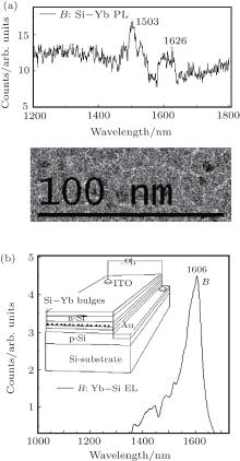
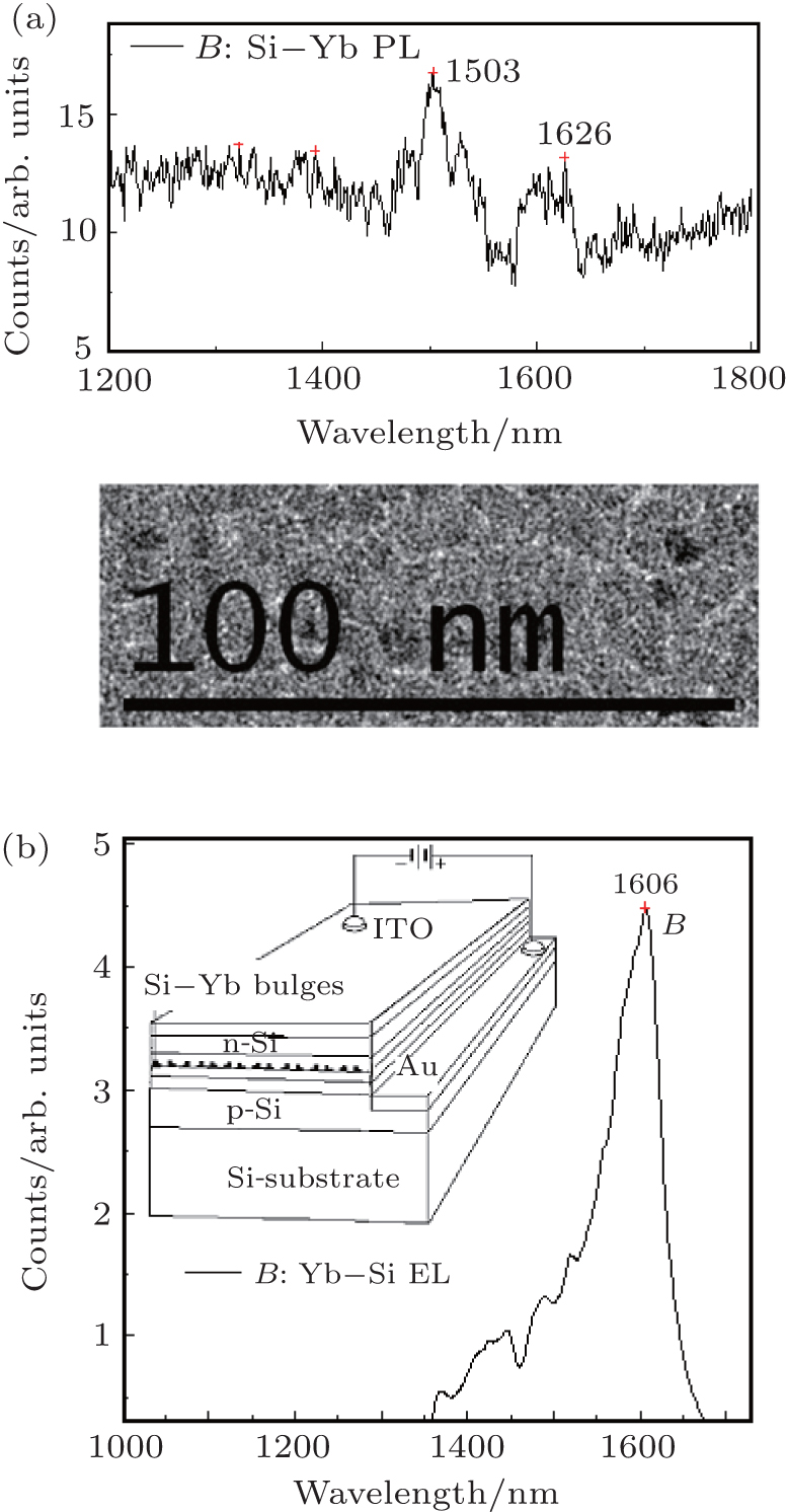 | Fig. 6. (a) PL spectrum on Si film coated by Yb, in which the peaks originating from the localized states of Si– Yb bond are observed in the telecom window, and the inset shows the bulge structure in TEM image of Si– Yb film. (b). EL spectrum on the emitter device of Si film coated by Yb, in which the enhanced EL emission near 1600 nm originates from the localized state of Si– Yb bond, and the EL device structure is shown in the inset scheme. |
The beam of the third harmonic of a pulsed Nd:YAG laser (wavelength: 355 nm, pulse width (FWHM): 20 ns, repetition rate: 1 kHz) is used as a pulsed laser deposition (PLD) laser to hit on Yb bar for depositing on Si film. The Yb bulges form on silicon film because of the strain produced from the mismatch between Si and Yb (the thickness of Yb film on Si film is about 10 nm), on which Si– Yb bonds could produce the localized states at deeper levels in band gap due to the curved surface effect[2] as well as Si= O bonds doing, even though there is no nanostructure on Si film whose Raman curve is shown in Fig. 3(b). In Fig. 6(a), PL peaks originating from the localized states of Si– Yb bonds are observed in the telecom window. Figure 6(b) shows the enhanced EL emission near 1600 nm originating from the localized state of the Si– Yb bond, in which the EL device scheme is shown in the inset of Fig. 6(b) (the Si– Yb quantum well and PIN hybrid junction with Si– Yb film structure are fabricated by using the method in Ref. [22]). Here, it is important that the localized state emission should originate from the Si– Yb bonds on the bulges in the gain layer of the device. It is easy to integrate the EL device on silicon chips for emission at the telecom wavelength.
Emission system with four-level construction like a laser level system will be built if the relaxation time of the localized states originating from surface bonds prepared by pulsed laser is long enough. Figure 7 shows the scheme of the four-level system, in which the localized states for visible light are built by some bonds on curved nanosilicon, such as Si– O– Si or Si= O bonds; and for emission in telecom window the
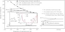
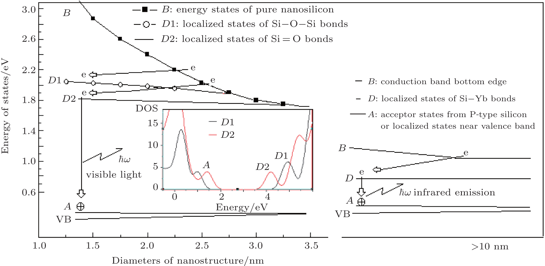 | Fig. 7. Scheme of the four-level system, in which the localized states for visible light could be built by some bonds on nanosilicon, such as Si– O– Si (D1) or Si= O bonds (D2); and for emission in telecom window the localized states could be build by doping with rare-earth atoms on Si film, such as Yb (D), and inset shows the calculation results that the two groups (D and A) of the localized states near conduction band and valence band in gap are respectively built on nanosilicon, and in the group D, the energy of the localized states D2 is lower than the energy of D1. |
localized states are built by depositing rare-earth atoms such as Yb on Si films. The inset in Fig. 7 shows the calculation results in the density of electronic states that the two groups (D and A) of the localized states near conduction band and valence band (VB) in gap are respectively built on nanosilicon, and in the group D showing that the energy of the localized states D2 is lower than the energy of D1. It should be noted that the perfect periodic structure provides the normal construction of the forbidden band, but some bonds on the curved surface of nanosilicon[22– 24] or on the surface bulges of Si film produced by plasmonic wave could break the symmetry of the system to cause the localized states to enter into gap, which has a longer relaxation time because of their position near the Fermi level.
The electronic behavior is investigated by an ab initio nonrelativistic quantum mechanical analysis in the work. It is found in the combination of the simulation calculation and the experimental results that the system energy is increased to build the emission centers of the localized states if the system symmetry is broken by the surface bonds on curved nanosilicons or bulges of Si film.
Our work demonstrates that the interaction and the coupling between plasmon and photon are built in the Purcell cavity of silicon by using a ns-pulsed laser, which generates the emission of the plasmonic standing wave in cavity, where the emission is observed by eyes or infrared camera. The plasmonic standing wave in the cavity could be used to fabricate various nanostructures in oxygen or nitrogen environment for visible light emission and to deposit rare-earth atoms on silicon film for emission in telecom wavelengths. The investigation of the PL spectra of the Si nanostructures prepared in oxygen or nitrogen environment and the EL spectra on the Si film coated by ytterbium develops a new way to manipulate emission wavelength. In the physical process, the interesting phenomena are observed, such as the plasmonic emission on standing wave structure produced by coupling with exciting photons in the cavity. The diffraction pattern on the plasmonic lattice structure is observed in the Purcell cavity of silicon, which is similar to the Wigner crystal structure. These results provide an interesting test bed to study complex process for preparing photonic material on silicon.
| 1 |
|
| 2 |
|
| 3 |
|
| 4 |
|
| 5 |
|
| 6 |
|
| 7 |
|
| 8 |
|
| 9 |
|
| 10 |
|
| 11 |
|
| 12 |
|
| 13 |
|
| 14 |
|
| 15 |
|
| 16 |
|
| 17 |
|
| 18 |
|
| 19 |
|
| 20 |
|
| 21 |
|
| 22 |
|
| 23 |
|
| 24 |
|