Plasma induced by pulsed laser and fabrication of silicon nanostructures

Plasma induced by pulsed laser and fabrication of silicon nanostructures |
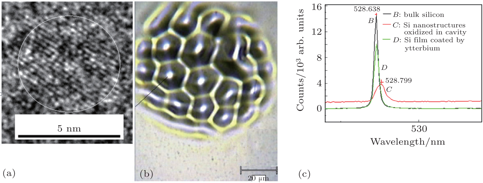
| (a) TEM image of Si nanostructure oxidized. (b) Optical image of hole-net structure prepared by the plasmonic standing wave induced by ns-pulsed laser at 355 nm in the cavity, in which the inset shows qunatum dot on nanosilicon in net-hole structure. (c) Raman scattering spectra, in which the curve B is the standard Raman spectrum on bulk silicon, and the curve C relates to the Si nanostructure. |
 |