|
|
Plasma induced by pulsed laser and fabrication of silicon nanostructures
|
Hang Wei-Qi† a) , Dong Tai-Ge b), Wang Gang b), Liu Liu Shi-Rong b), Huang Zhong-Mei a), Miao Xin-Jian a), Lv Quan c), Qin Chao-Jian b) |
|
| |
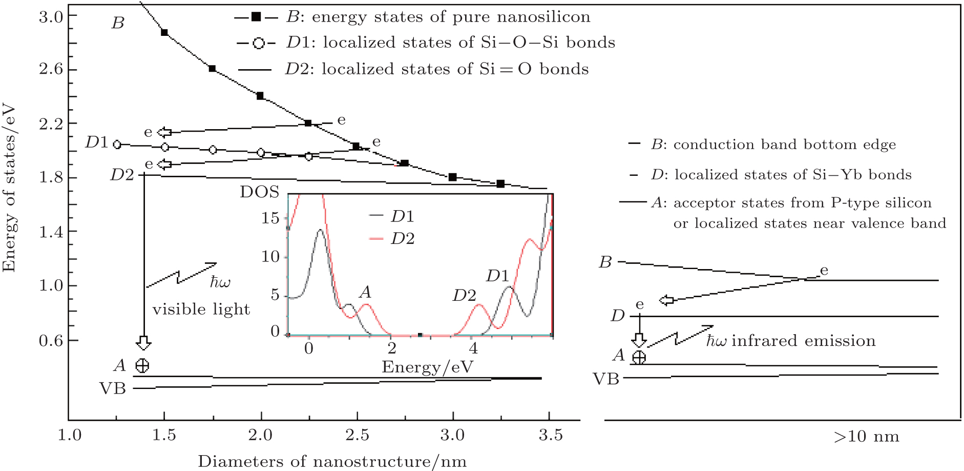
| Scheme of the four-level system, in which the localized states for visible light could be built by some bonds on nanosilicon, such as Si–O–Si ( D 1) or Si=O bonds ( D 2); and for emission in telecom window the localized states could be build by doping with rare-earth atoms on Si film, such as Yb ( D ), and inset shows the calculation results that the two groups ( D and A ) of the localized states near conduction band and valence band in gap are respectively built on nanosilicon, and in the group D , the energy of the localized states D 2 is lower than the energy of D 1. |
|
|
 |
|
|