Plasma induced by pulsed laser and fabrication of silicon nanostructures

Plasma induced by pulsed laser and fabrication of silicon nanostructures |
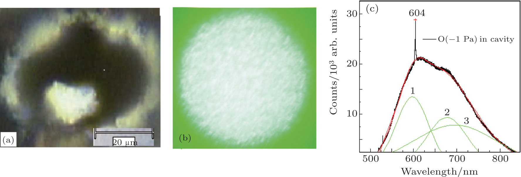
| (a) Optical image of the plasmonic emission on the oxidized Si nanostructures excited by a xenon lamp in the cavity. (b) Optical image of the plasmonic emission on the oxidized Si nanostructures under the 514-nm excitation of an argon ion laser in the cavity. (c) PL spectrum on the sample (Fig. 3(a) ) after annealing treatment, in which there is a sharp peak at 604 nm (optical gain coefficient > 80). |
 |