|
|
Plasma induced by pulsed laser and fabrication of silicon nanostructures
|
Hang Wei-Qi† a) , Dong Tai-Ge b), Wang Gang b), Liu Liu Shi-Rong b), Huang Zhong-Mei a), Miao Xin-Jian a), Lv Quan c), Qin Chao-Jian b) |
|
| |
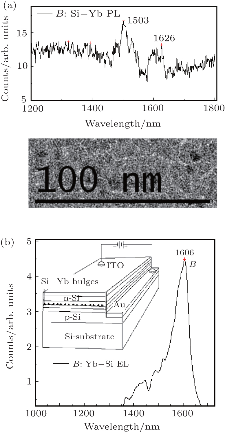
| (a) PL spectrum on Si film coated by Yb, in which the peaks originating from the localized states of Si–Yb bond are observed in the telecom window, and the inset shows the bulge structure in TEM image of Si–Yb film. (b). EL spectrum on the emitter device of Si film coated by Yb, in which the enhanced EL emission near 1600 nm originates from the localized state of Si–Yb bond, and the EL device structure is shown in the inset scheme. |
|
|
 |
|
|