


Relationship between bias voltage and microstructure as well as properties of CrAlYN films*
[Fu Ying-Yinga), b) , Li Hong-Xuana) , Ji Lia)  , Liu Xiao-Hong
a) , Liu Liuc) , Zhou Hui-Dia) , Chen Jian-Mina) ]
, Liu Xiao-Hong]
|
|

 , Liu Xiao-Hong
†Corresponding author. E-mail: jili@licp.cas.cn
Corresponding author. E-mail: Chenjm@licp.cas.cn
*Project supported by the National Basic Research Program of China (Grant No. 2013CB632302) and the National Natural Science Foundation of China (Grant No. 51175491).
In this work, a series of CrAlYN films doped with 1 at.% yttrium were deposited by unbalanced reactive magnetron sputtering under different bias voltages. The effects of bias voltage on microstructure and properties of the CrAlYN films were subsequently investigated. It is found that all the as-deposited films have similar chemical composition and crystalline structure. However, the bias voltage has significant impact on the mechanical properties and oxidation resistance of the resulting films. Namely, the film deposited at 100 V has the highest hardness and best oxidation resistance, which are mainly attributed to its denser structure and higher Al content than others. In addition, the film obtained at 100 V exhibits superior oxidation resistance even at 1000 °C, and good friction and wear properties at 600 and 800 °C, and the latter two are mainly ascribed to the formation of compact transfer layer on the worn surfaces. However, this film experienced obvious wear loss at low testing temperatures (i.e., 200 and 400 °C) due to the serious abrasive wear.
With the rapid development of modern industry, nitride films (e.g., TiN, CrN, etc.) are widely used for various purposes in recent years due to their promising thermal stability and corrosion resistance together with good tribological properties.[1– 4] Comparing with binary CrN films, the oxidation resistance of ternary CrAlN films was significantly improved up to 900 ° C due to the formation of oxide scales on the film surface during annealing treatment. The oxides can effectively restrain the inward and outward diffusions of oxygen and metallic cations to some extent.[5– 7] However, previous studies have shown that the metastable fcc CrAlN films will completely fail once the working temperature exceeds 900 ° C, which does not meet the demand of high-speed cutting application, where the temperature at the cutting edges can exceed 1000 ° C. Many efforts have been made to further promote the oxidation resistance of CrAlN films, and lots of researches have shown that a small amount of Y incorporated into CrAlN films can effectively increase the oxidizing temperature up to 1000 ° C.[8, 9] The improved oxidation resistant behaviors of CrAlN film by adding Y are attributed to the enhanced adhesion of oxide scales and the formation of Y oxide complexes at the grain boundaries, blocking the fast diffusion paths.[10] Besides, the addition of Y can also improve the mechanical properties and prevent the grain coarsing at elevated temperatures.[9, 11] At present, the influence of Y content on the microstructure, chemical composition, and properties of CrAlN film have been considerably investigated, and it has been proved that the optimal Y doping content in CrAlN film is around 1 at.% for obtaining superior performances.[8, 12, 13] For instance, Rovere et al. systemically studied the effect of Y content on the oxidation resistance of CrAlN films, and found that an excellent oxidation resistance was obtained with Y content of 1 at.% in CrAlYN film, while the film had a poor oxidation resistance once the Y fraction exceeds 2 at.%.[8] Rojas et al. investigated the oxidation resistant behaviors of CrAlYN film with 1.7 at.% Y, and pointed out that the studied film exhibited excellent oxidation resistance up to 1000 ° C.[12] Qi et al. found that the oxidation resistance of the CrAlYN films significantly decreased as Y content was not less than 1.3 at.%.[13] Inspired by these existing results, the later works mainly focused on the microstructure and performances of CrAlYN film with ∼ 1 at.% Y. However, less research about the influence of bias voltage on CrAlYN film was reported even though it has been proved that the bias has important effect on film microstructure and performances.[14– 16] Moreover, a majority of researches about CrAlYN films mainly focused on their mechanical properties and oxidation resistance, while the tribological properties of the films, especially for the high-temperature tribological performances, were less reported.
In this work, the relationship between bias voltage and microstructure as well as properties of CrAlYN film is investigated in order to understand how to optimize the overall properties of the CrAlYN film by adjusting the bias voltage to achieve a good thermal stability and tribological properties. It is worth mentioning that the oxidation resistance and tribological properties at elevated temperatures are mainly investigated, and the friction and wear mechanisms are discussed in detail.
The CrAlYN films were deposited on silicon (111) wafer and high-temperature alloy steel (GH4169) substrates by using medium frequency unbalanced reactive magnetron sputtering system at different bias voltages. The high-temperature alloy steel samples were used for mechanical, thermal, and tribological characterizations, and other properties were tested with silicon samples. The deposition system was described in detail elsewhere.[17] High-purity Ar (99.99%) and N2 (99.99%) mixture gases were used as the sputtering gases and two Cr targets (99.8%) as well as one AlY alloy target (99.5%, Y: 10 wt.%) were employed as sputtering sources. A medium frequency alternating current power supply (40 kHz) was connected to two Cr targets, and a direct current power supply was connected to AlY alloy target to control the sputtering current. The substrates were ultrasonically cleaned in deionized water, acetone, and alcohol for 15 min successively before they were put into the deposition chamber. All the substrates were placed parallel to the targets at a distance of 100 mm. Before deposition, the chamber was heated up to 100 ° C, and meanwhile a base pressure of about 4× 10− 3 Pa was attained by a turbo molecular pumping system. Subsequently, the substrates were etched with Ar+ ions in the chamber under a bias voltage of − 600 V at a pressure of 1.4 Pa for 20 min to remove the native oxides and contamination on the substrates surface. Then, a chromium interlayer of about 200 nm thick was predeposited to improve adhesion between final film and substrate. Finally, a series of CrAlYN films about 2.3 μ m thick were deposited at different bias voltages (absolute value), ranging from 75 to 175 V, under a working gas pressure about 0.34 Pa. The detailed deposition parameters are listed in Table 1.
Film thickness was measured by a 3D non-contact surface profilometer (Micro-XAM, USA). The chemical compositions of the films were determined by electron probe microanalysis (EPMA-1720, Shimadzu, JPN) under an acceleration voltage of 15 kV and beam size of 10 μ m. The instrument was firstly calibrated by Cr2O3 (synthetic, 99.7%), Y3Al5O12 (synthetic, 99.9%), and BN (pyrolytic, Corp., USA) before sample testing. The crystalline structure of the films was studied by conventional Bragg– Brentano x-ray diffraction (XRD) using a Philips X’ Pert-MRD type diffractometer with a Cu tube operated at 40 kV and 60 mA under a glancing angle of 2° at a scanning speed of 5° /min. The cross-sectional structure and surface morphology of the deposited films were studied by field emission scanning electron microscopy (FESEM). In this study, residual stress of samples can be calculated with the following Stoney equation:[18]

where σ is the internal stress, R1 and R2 are the substrate curvature radii before and after the film deposition, ν s and Es are the Poisson’ s ratio and the Young’ s modulus of the substrate, ts and tf are the thicknesses of the substrate and the film, respectively. The mechanical properties of the films were determined using a NanoTest 600 nanomechanical system (Micro-Materials Ltd, UK), and ten repeated indentations were made for each sample with the same condition. The crystalline microstructure, hardness, and the cross-section structure of the CrAlYN films after annealing treatment were also analyzed by above-mentioned characterization techniques. The oxidized film was firstly mechanically cut into little pieces and then embedded in the epoxy resins in order to protect the cross section during the process of mechanical polishing.
| Table 1. Deposition parameters for CrAlYN films. |
The oxidation resistance of the studied films was estimated at desired temperature in air atmosphere for 2 h by using a muffle furnace with heating rate of 5 ° C/min. All the samples deposited at various bias voltages were evaluated under 1000 ° C, and the sample obtained at 100 V was specially tested from 800 to 1100 ° C for its better oxidation resistance than others. The tribological properties were tested by a ball-on-disk high-temperature tribometer (CSM, Switzerland) at 200, 400, 600, and 800 ° C in air. Al2O3 balls with diameter of 6 mm were used as counterparts. The sliding distance, average speed, normal load, and the radius of the wear track were 100 m, 5 cm/s, 2 N, and 5 mm, respectively. The friction tests were carried out three times for each film under each studied temperature. Non-contact 3D surface profilometry (Micro, XAM, USA) was used to measure wear volume.
Table 2 shows the chemical composition, obtained by EPMA analysis, of CrAlYN films prepared at different bias voltages. It is found that all the films are non-stoichiometric with an excess of metal or nitrogen atoms. The Al concentration in the films firstly increases from 25.0 to 27.0 at.% as the bias voltage increases from 75 to 100 V, and then decreases to 24.1 at.%, while the bias voltage further increases to 175 V. The increased Al fraction with increasing bias voltage from 75 to 100 V is probably attributed to the enhanced adatom diffusion caused by moderate ion energy.[19, 20] However, when the bias voltage is higher than 100 V, the gradual reduction of the fraction of Al in films is due to the preferential sputtering of the lighter Al atom than Cr and Y atoms.[21, 22] The excess of N compared to metal atoms in films with increase of bias voltage from 125 to 175 V may be ascribed to the fact that more and more N atoms are ionized and implanted into film under the action of high bias voltage. The Y content almost keeps a constant value about 1.0 at.% in all films except for the case of 75 V, suggesting that the bias voltage has little influence on Y. In addition, the Al/Cr ratio has a maximum value of 1.17 at 100 V and a minimum value of 0.94 at 75 V, while others are 1.1.
| Table 2. Composition of the CrAlYN films deposited at different bias voltages. |
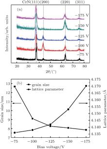
The crystalline structures of the CrAlYN films deposited at various bias voltages were studied by XRD, and the corresponding results are presented in Fig. 1. It can be seen from Fig. 1(a) that the bias voltage has no significant influence on the crystal structure of the resultant films, and all the films exhibit a single phase of fcc CrAlYN crystalline structure with typical diffraction peaks of (111), (200), (220), and (311). No peaks belonging to crystalline hcp-AlN were detected due to the low Al concentration (ranging from ∼ 24 to 27 at.% in the film), which is lower than the limit of Al solubility in the fcc-CrN lattice.[23– 27] The average grain size and the lattice parameter of the (111) peak as a function of bias voltage are also given in Fig. 1(b). As the bias voltage increases, the grain size gradually decreases, while the lattice parameter increases gradually, similar experimental result was also observed by others.[16] The reduced grain size at high bias voltage is due to the intensive bombardment of incident ions with high kinetic energy, which would generate more nucleation sites such as defects on the growing film surface, and hence decrease the grain size.[15, 28] Besides, it also can be seen that the peaks of (111) and (220) shift to lower 2θ angle once the bias higher than 100 V, indicating an increase of lattice parameter and internal stress in the films.[29] Moreover, it is noted that the full width at half maximum (FWHM) of the (111) peak increases with increasing bias voltage, which is ascribed to the decrease of grain size and increase of microstrain.[20, 30] The influence of microstrain on FWHM is neglected in this study since the microstraining effect is relatively small and can be ignored when calculating the grain size according to Zhang et al. and Basnyat et al.[31, 32]
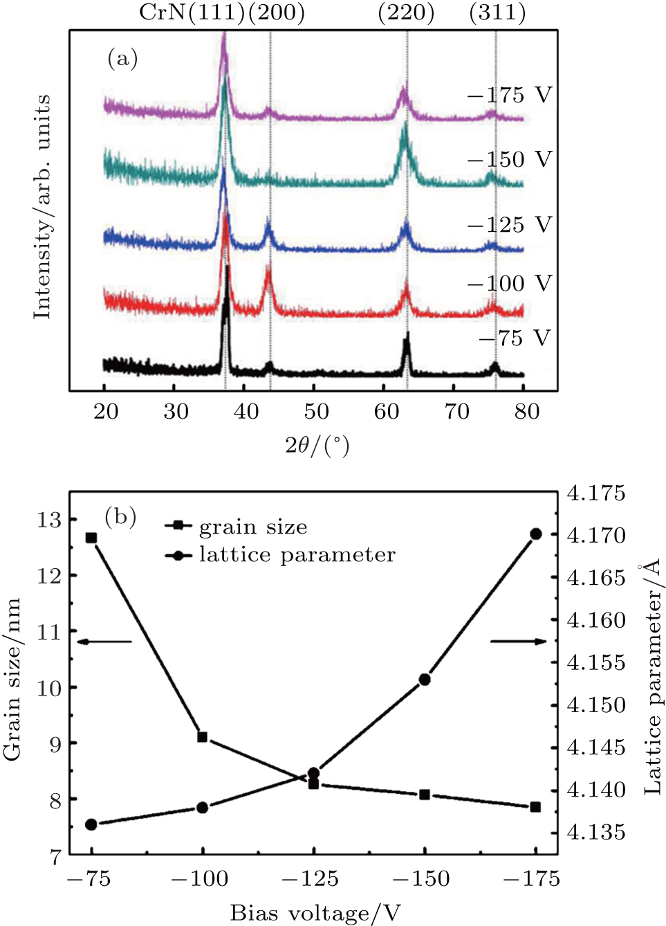 | Fig. 1. XRD patterns (a) and grain size as well as lattice parameters (b) of CrAlYN films deposited under different bias voltages. |
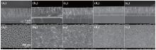
Figure 2 shows the typical FESEM cross-sectional and surface morphologies of the CrAlYN films deposited under different bias voltages. The cross-sectional microstructures of all the films has typical columnar characteristic lying in the zone T of Thornton model.[33] A very porous, open columnar, and pyramid-like surface structure is obtained for film deposited at low bias voltage of 75 V. For films deposited at 100 and 125 V, the open boundaries between columnar crystals disappear, while dense and leafy film surfaces are achieved. As for the films deposited at higher bias voltages such as 150 and 175 V, they exhibit similar surface features, which can be described as cauliflower-like one. The morphology evolution with bias voltage is likely to be connected with the ion energy/ion flux changes during film deposition processes. At the low bias voltage of 75 V, the incident ion flux with low energy leads to low nucleation density due to the low mobility of the adatoms on the surface, and hence a coarse columnar cross-section and a porous surface are obtained. The high incident ion energy/flux at high bias voltage results in an increased mobility of the adatoms and a higher nucleation density, and thus denser structure is achieved. Besides, highly migratory adatoms can move or diffuse into the inter-grain voids under the high-energy ion bombardment, leading to the formation of denser structure.[19, 34, 35] Moreover, the energetic ion bombardment on the growing film can elevate the film surface temperature, which is helpful to increase the atom mobility, thereby more denser structure is obtained.[35, 36]
The evolution of mechanical properties of CrAlYN films as a function of bias voltages is given in Fig. 3. It can be seen from Fig. 3(a) that all the films exhibit compressive stress. The absolute value of compressive stress increases from 0.15 to 0.59 GPa as the bias voltage increases from 75 to 150 V, and then the compressive stress keeps almost constant when the bias voltage further increases to 175 V. The hardness increases sharply from 7.6 to 24.6 GPa when the bias voltage elevates from 75 to 100 V, and then decreases to some extent as the bias voltage further increases. The gradual increase in compressive stress with bias voltage ranging from 75 to 150 V is mainly due to the increase in the ion peening effect.[37] This effect leads surface atoms to be knocked into interstitial sites in the near surface region, accompanied by a local atomic rearrangement. As a result, the internal stress was formed in films.[15] However, the compressive stress almost keeps constant when the bias voltage further increases to 175 V, which is due to the lattice relaxation induced by the heating effect resulting from energetic ion bombardment.[15, 16] The hardness of film is affected by several factors, such as grain size, microstructure, internal stress, the chemical composition, etc. The improved hardness as the bias voltage increases to 100 V is mainly attributed to the quick decrease of grain size from 12.7 to 9.1 nm (see Fig. 1(b)) and the increase of compressive stress (see Fig. 3(a)). The reduced grain is the main reason for the enhanced film hardness since the number of dislocations piled up against a grain boundary decreases, as described by Hall– Petch relationship.[14] Besides, the increase of compressive stress results in promoting film hardness due to the formation of lattice defects, which hinders dislocation movements.[38] However, according to Ma et al.[39] and Qi et al., [40] the inverse Hall– Petch effect can appear in CrN film at the grain size of 11.4– 12.5 (theoretical value) and 10.0– 16.0 nm (experimental value), respectively. Once the grain size is less than this critical value, the film hardness will decrease with further decrease of grain size. However, it is important to point out that the grain size calculated from Scherrer’ s equation is several nanometers smaller than the one obtained from single-line method.[40] Moreover, in this study, the hardness increases as the grain size decreases from 12.7 to 9.1 nm, indicating that this value does not exceed the critical value. It is therefore reasonable to infer that the inverse Hall– Petch effect does not work in this case. Additionally, the highest Al content (27.02 at.%) in film deposited at 100 V also contributes to its highest hardness due to the greatest contribution of covalent Al– N bonds.[3] The grain size decreases to ∼ 7.5 nm and the compressive stress further increases to ∼ 0.6 GPa when the bias voltage increases to 175 V, and hence the film hardness should further increase according to the Hall– Petch effect. Actually, the hardness decreases to some extent probably due to the further decrease of grain size whose value might reach the critical value and the inverse Hall– Petch effect plays an important role on the hardness decrease. As the grain size changes in a very narrow range from 8.2 to 7.5 nm with increasing bias from 150 to 175 V, the effect of inverse Hall– Petch effect on the film hardness can be ignored. Therefore, the reasons for hardness enhancement as the bias is higher than 125 V are mainly attributed to the higher compressive stress and the denser microstructure. According to previous studies, [41, 42] the H/E and H3/E2 are strongly associated with film performance, and at present the relatively high H/E (close to 0.1) and H3/E2 (close to 0.20) ratio indicate that the resulting films have high elastic strain to failure ability and good ability to resist plastic deformation.
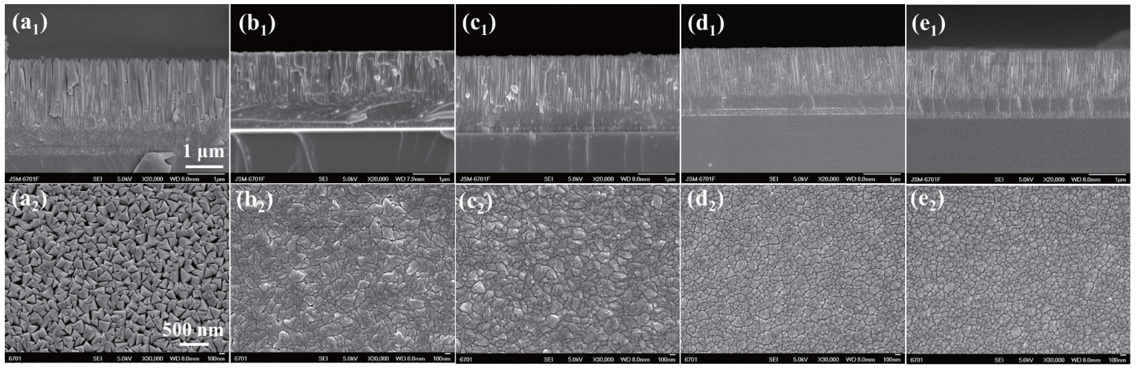 | Fig. 2. Typical FESEM cross-sectional and surface morphologies of the CrAlYN films deposited under different bias voltages (a1, a2) − 75 V, (b1, b2) − 100 V, (c1, c2) − 125 V, (d1, d2) − 150 V, and (e1, e2) − 175 V. |
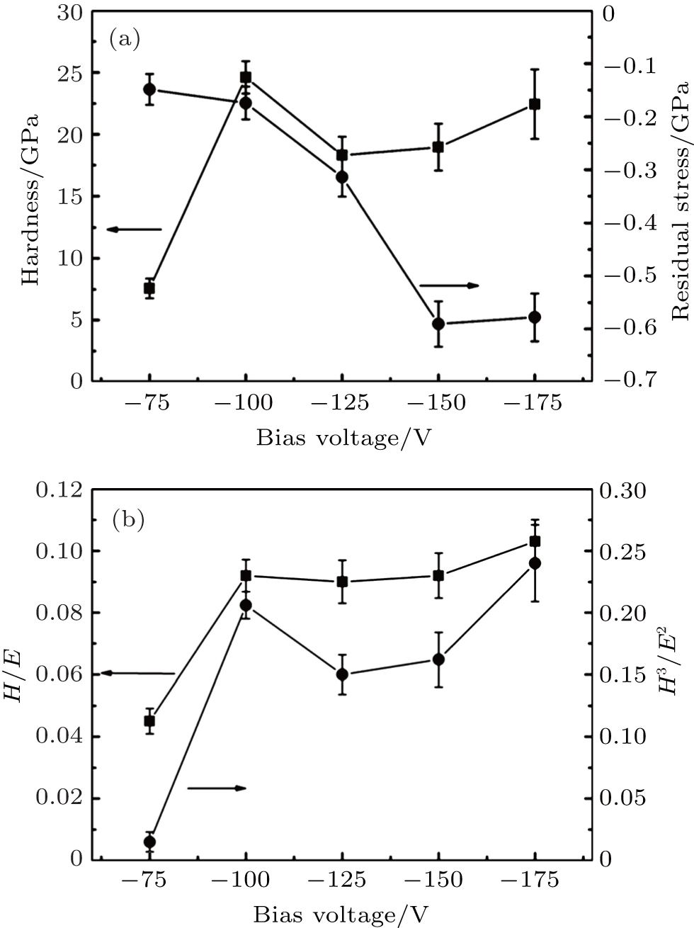 | Fig. 3. Hardness and residual stress (a), and H/E as well as H3/E2 (b) of the CrAlYN films deposited under different bias voltages. |
For hard films, good oxidation resistance and excellent hot hardness are very crucial for their practical applications since they are often exposed in high temperature conditions during normal operation period. Hence, the oxidation resistance of the CrAlYN films was evaluated by XRD and nano-indentation techniques. Figure 4(a) shows the XRD patterns for the CrAlYN films deposited at different bias voltages after annealing at 1000 ° C in air for 2 h in a muffle furnace. For film deposited at 75 V, except for the original film peaks, a strong peak around 36.11° and several weak peaks (located at 50.10° , 54.68° , and 64.9° , respectively) corresponding to Cr2O3 are found in the diffraction patterns, indicating that this film is severely oxidized. The poor oxidation resistance for this film is ascribed to its porous and coarse columnar microstructure, which supply paths for outward diffusion of metal and nitrogen as well as inward diffusion of oxygen during thermal treatment.[13, 43] For films prepared under bias voltages of 100 and 125 V, a relatively obvious peak of Al2O3 is discovered at 41.90° , while other oxidation peaks are very weak, especially for the one deposited at 100 V, demonstrating a good oxidation resistant behavior of the films. The probable reason for the good oxidation resistance for this film is the more compact microstructure compared with the one deposited at 75 V, which is conducive to retard oxygen diffusion and hence improve the oxidation resistance of the film to some extent. Furthermore, the highest Al content for film deposited at 100 V also contributes to its better oxidation resistance as the stronger covalent Al– N bond helps to suppress film decomposition at elevated temperature.[44] Obvious peak of Al2O3 is found at 37.91° and weaker peaks of Cr2O3 are observed at 36.11° and 40° for films deposited at 150 and 175 V, respectively, indicating that these films were oxidized to some extent. It was expected that the more compact microstructure for films deposited at 150 and 175 V, compared with the film prepared at 100 V, should be beneficial for achieving better oxidation resistance. However, the relatively lower Al content together with higher compressive stress, associating with more defects, [44, 45] are the dominant reasons for their poor oxidation resistance.
 | Fig. 4. XRD patterns for the CrAlYN films deposited at different bias voltages after annealing at 1000 ° C for 2 h (a), and for film deposited at − 100 V after annealing from 800 to 1100 ° C (b). |
The oxidation resistant behaviors for film deposited at 100 V at elevated temperatures from 800 to 1100 ° C are also investigated, and the XRD patterns are given in Fig. 4(b). The XRD patterns after annealing at 800 ° C even at 900 ° C are similar to the as-deposited one, as shown in Fig. 1(a), indicating that no significant structure changes occur at the corresponding annealing temperatures. With the increase of annealing temperature up to 1000 ° C, a weak peak corresponding to Cr2O3 and a strong peak belonging to α -Al2O3 are found at 36.11° and 41.90° , respectively, suggesting that the film is oxidized to some extent. Several oxidation peaks belonging to α -Al2O3 (25.70° , 35.37° , 41.90° ), θ -Al2O3 (39.80° , 67.58° , 75.02° ), and Cr2O3 (24.56° , 33.61° , 36.11° ) are found for film annealed at 1100 ° C, manifesting that the film was oxidized severely. It is worth noting that the CrAlYN film exhibits better oxidation resistance even at 1000 ° C compared with our previous CrAlN film.[46, 47] The latter was significantly oxidized at 800 ° C. The reasons for the improved oxidation resistance of present CrAlYN film are the enhancement adhesion of oxide scales and the formation of Y oxide complexes at the grain boundaries, blocking the fast diffusion paths for oxygen.[10]
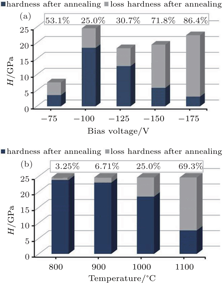
The mechanical properties of CrAlYN films after annealing treatment are investigated detailedly, and the corresponding results are given in Fig. 5. It can be clearly seen from Fig. 5(a) that compared with the original films, hardness of all the studied films decreases more or less after annealing treatment at 1000 ° C. The oxidation resistance of CrAlYN films plays an important role on the film hardness loss after annealing treatment. Namely, after being annealed, the film with good oxidation resistance has little reduction in hardness, but the film with poor oxidation resistance shows an obvious reduction in hardness. Here, the film with the best oxidation resistance still maintains a high hardness about 18.4 GPa after annealing treatment. To further investigate the effect of annealing treatment on the mechanical properties of the CrAlYN film, we take the film deposited at 100 V as an example to study the evolution of hardness as a function of annealing temperature. It can be seen from Fig. 5(b) that the film hardness decreases slightly with the increase of annealing temperature from 800 to 1000 ° C, and then decreases significantly once the temperature exceeds 1000 ° C. The hardness reduction with the increase of annealing temperature in the range from 800 to 1000 ° C is owing to the residual stress recovery, defect annihilation, recrystallization, and a growth of the grain during annealing process.[48– 52] Moreover, the formation of thin oxide layer on the film surface during annealing treatment is responsible for the reduced film hardness. The sharp reduction in hardness once the annealing temperature exceeds 1000 ° C may be due to the significant increase of oxide thickness to a level capable of being detected by XRD technique, as shown in Fig. 4. The percent of hardness loss is also given in Fig. 4, which can intuitively reflect the degree of hardness loss of the film after annealing at different temperatures.
 | Fig. 5. Hardness for the CrAlYN films deposited at different bias voltages after annealing at 1000 ° C for 2 h (a), and for film deposited at 100 V after annealing from 800 to 1100 ° C (b). |
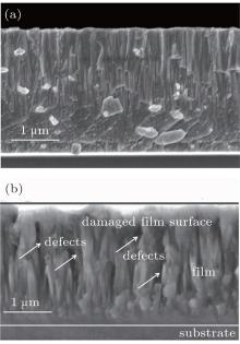
To further analyze the influence of annealing treatment on microstructure and mechanical properties of the thin film, the typical FESEM cross-sectional images of CrAlYN film before and after annealing at 1000 ° C are shown in Fig. 6. It is observed from Fig. 6(a) that the as-deposited film has compact microstructure and fine grains. However, a large number of defects inside the film are found after annealing treatment. Those defects were generated due to excess vacancy annihilation, grain boundary relaxation, shrinkage of grain-boundary voids, and recrystallization. Moreover, the outward diffusion of metal cations (Cr3 + , Al3 + ) and inward diffusion of anions (O2− ) and electrons (e− ) through the oxide layer result in the accumulation of holes (h+ ) and subsequent formation of pores/defects at the film/oxide interface.[10] Therefore, these defects in the oxidized film are mainly responsible for the hardness reduction compared with as-deposited film. In addition, it is found that the thickness of CrAlYN film after annealing is thinner than that of as-deposited film, which is due to the destruction of the surface oxide layer during the process of sample preparation.
 | Fig. 6. Typical FESEM cross-sectional images for as-deposited CrAlYN film at -100 V (a), for film after annealing at 1000 ° C for 2 h (b). |
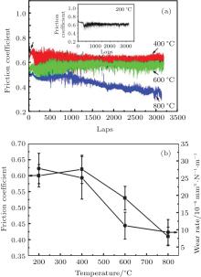
The high-temperature tribological properties of CrAlYN film deposited at 100 V were systemically investigated, and the friction coefficient curves of film under different temperatures are given in Fig. 7(a). After a short running-in period, the friction coefficient curve at 800 ° C has some fluctuation while relatively stable curves are obtained under other tested temperatures. The average friction coefficient and wear rate of the studied CrAlYN film as a function of testing temperature are displayed in Fig. 7(b). The friction coefficient increases slightly from 0.60 to 0.62 as the temperature increases from 200 to 400 ° C, and then gradually decreases to 0.41 when the temperature further increases to 800 ° C. The highest wear rate of 2.78× 10− 5 mm3· N− 1· m− 1 and the lowest one of 9.29× 10− 6 mm3· N− 1· m− 1 are obtained at 200 and 800 ° C, respectively.
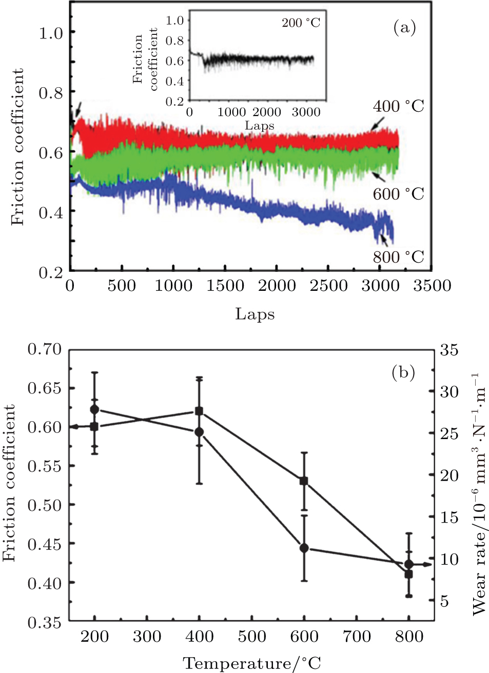 | Fig. 7. Friction coefficient curves (a) and average wear rates (b) of CrAlYN film tested under different temperatures. |
To gain more insight into friction and wear mechanisms of the resulting CrAlYN film under high temperature, the worn surfaces of both film and Al2O3 ball were studied by SEM and 3D surface profiler, and the corresponding results are given in Figs. 8 and 9. The worn surface of CrAlYN film at 200 ° C is featured by a large amount of loose wear debris (see Fig. 8(a1)). The worn surface is very rough and lots of furrows are observed thereon, and the wear depth is very different from one point to another (see Fig. 8(a2)), indicating that the film suffered a serious abrasive wear. When the testing temperature increases to 400 ° C, the wear debris on the wear track is relatively fine and evenly distributed on the worn surface (see Fig. 8(b1)), and the wear depth is comparatively uniform along the track (see Fig. 8(b2)). By further increasing the testing temperature to 600 even 800 ° C, the wear tracks are smooth and the wear debris formed a discontinuous compact layer in the middle of the wear track (see Figs. 8(c1) and 8(d1)). Meanwhile, the furrows are narrower and shallower compared with the ones obtained at 200 and 400 ° C (see Figs. 8(c2) and 8(d2)). Additionally, the two sides of wear tracks are higher than the original film surface to some extent, suggesting that an adhesive wear occurs during friction period. The Al2O3 balls sliding against the CrAlYN films under 200 and 400 ° C have very rough worn surfaces and large wear scar diameters (see Figs. 9(a1)) and 9(b1)), indicating that the balls suffered severe wear. Besides, obvious transferred materials are found on the worn surfaces. As the testing temperature increases, the worn surfaces of balls become more and more smooth (see Figs. 9(c1)) and 9(d1)), and some laminar transfer materials with high Cr content are observed, especially for the one obtained at 800 ° C (see Fig. 9(d2)), indicating that an adhesive wear occurs.
According to the above tests and characterization, it can be inferred that at low temperatures of 200 and 400 ° C, the wear loss of the counterpart surfaces during the running-in period generated large amounts of hard wear debris, part of which are dispersed at the edges of wear tracks, and part of which are entrapped in the sliding interfaces. The entrapped wear debris would further plow the sliding interfaces during the next friction period, leading to the formation of furrows and rough worn surfaces. As a result, high friction and wear are obtained. The high friction coefficients and wear rates for film tested at 200 and 400 ° C may be due to the removal of condensed water vapor from the sliding surfaces.[47] In contrast to the low temperatures of 200 and 400 ° C, soft oxides are easily formed on the sliding surfaces at the beginning of friction test under higher testing temperatures of 600 and 800 ° C. In the next friction process, these soft oxides with low shear strength can be easily sheared off by counterpart ball to form wear debris. Different from the low temperature cases, in high temperature condition, the soft wear debris entrapped between sliding interfaces were further broken into finer wear debris, which would agglomerate into clusters and adhere to the parent worn surface, leading to the formation of a discontinuous transfer layer attached on the worn surface. This transfer layer partially separates the mated ball and the film surface, and hence low friction and wear are obtained at high temperatures.
The CrAlYN films were deposited with different bias voltages using unbalanced reactive magnetron sputtering system in this study. Although the bias voltage has trivial influence on the film composition and crystalline structure, the film deposited at 100 V has the highest hardness among all the studied films, which is ascribed to the relatively compact structure and high Al content. When the bias is higher than 100 V, the hardness decreases to some extent due to the inverse Hall– Petch effect works in this condition. The reasons for hardness enhancement as the bias is higher than 125 V are mainly attributed to the higher compressive stress and the denser microstructure. The oxidation resistance of CrAlYN films is also bias dependent, and the XRD analysis demonstrates that the film deposited at 100 V is free from oxidation even though it is annealed at 900 ° C, which is ascribed to the more compact microstructure and higher fraction of covalent Al– N bond compared to the one deposited at 75 V. For films deposited at higher bias, the relatively lower Al content, higher compressive stress, and more defects are the dominant reasons for their poor oxidation resistance. Tribological properties of CrAlYN film are temperature-dependent. The CrAlYN film suffered severe wear at 200 and 400 ° C due to the abrasive wear. However, under elevated temperatures of 600 and 800 ° C, the films exhibit good tribological properties with low friction and wear. The formation of compact transfer film is mainly responsible for the good tribological properties in those cases.
 | Fig. 8. SEM and three-dimensional images of worn surfaces of CrAlYN films tested under different temperatures of 200 ° C ((a1), (a2)), 400 ° C ((b1), (b2)), 600 ° C ((c1), (c2)), and 800 ° C ((d1), (d2)). |
 | Fig. 9. SEM wear morphologies and EDS elemental distributions of worn surfaces for Al2O3 balls under different temperatures of 200 ° C ((a1), (a2)), 400 ° C ((b1), (b2)), 600 ° C ((c1), (c2)), and 800 ° C ((d1), (d2)). |
| 1 |
|
| 2 |
|
| 3 |
|
| 4 |
|
| 5 |
|
| 6 |
|
| 7 |
|
| 8 |
|
| 9 |
|
| 10 |
|
| 11 |
|
| 12 |
|
| 13 |
|
| 14 |
|
| 15 |
|
| 16 |
|
| 17 |
|
| 18 |
|
| 19 |
|
| 20 |
|
| 21 |
|
| 22 |
|
| 23 |
|
| 24 |
|
| 25 |
|
| 26 |
|
| 27 |
|
| 28 |
|
| 29 |
|
| 30 |
|
| 31 |
|
| 32 |
|
| 33 |
|
| 34 |
|
| 35 |
|
| 36 |
|
| 37 |
|
| 38 |
|
| 39 |
|
| 40 |
|
| 41 |
|
| 42 |
|
| 43 |
|
| 44 |
|
| 45 |
|
| 46 |
|
| 47 |
|
| 48 |
|
| 49 |
|
| 50 |
|
| 51 |
|
| 52 |
|