† Corresponding author. E-mail:
Project supported by the National Natural Science Foundation of China (Grant No. 61774052) and the Excellent Youth Foundation of Zhejiang Province, China (Grant No. LR17F040001).
In this paper, we propose a new enhanced GaN MISFET with embedded pn junction, i.e., EJ-MISFET, to enhance the breakdown voltage. The embedded pn junction is used to improve the simulated device electric field distribution between gate and drain, thus achieving an enhanced breakdown voltage (BV). The proposed simulated device with LGD = 15μm presents an excellent breakdown voltage of 2050 V, which is attributed to the improvement of the device electric field distribution between gate and drain. In addition, the ON-resistance (RON) of 15.37 Ω ⋅mm and Baliga’s figure of merit of 2.734 GW⋅cm−2 are achieved in the optimized EJ-MISFET. Compared with the field plate conventional GaN MISFET (FPC-MISFET) without embedded pn junction structure, the proposed simulated device increases the BV by 32.54% and the Baliga’s figure of merit is enhanced by 71.3%.
Gallium nitride (GaN)-based electronic devices have become one of the most promising candidates for power applications. Owing to the strong polarization charge in the AlGaN/GaN hetero-junction, high-density two-dimensional electron gas (2DEG) is formed at the interface between GaN and AlGaN.[1–5] It has drawn intensive attention for high voltage applications due to its wide band gap. However, it is still a challenge to improve the breakdown voltage.[6] Like the scenario in LDMOS, the peak electric field in GaN MISFET is distributed in the device surface. Chen has made a great contribution to the development of power device, and he proposed a composite buffer layer structure which was called COOLMOSTM.[7] Moreover, theoretical analysis on the structure was reported in detail, and the structure was also called the super junction. The super junction concept was also known as super multi-RESURF.[8] So, the technologies of RESURF were widely applied to power devices. Back electrode has been used to realize RESURF GaN HEMT in Ref. [9]. Field plate is also a common method to improve the electric field distribution.[10] Source field plates, gate field plates, and drain plates were used to improve the electric field distribution between gate and drain.[11–15] Some researchers demonstrated the GaN-based super HFETs based on polarization junction concept and they have great power characteristics.[16] Some researchers proposed a novel enhancement-mode polarization-junction HEMT with vertical conduction channel which has a uniform electric field distribution between source and drain.[17] Some researchers proposed and experimentally demonstrated a high-breakdown-voltage HEMT by implanting fluorine ions in a thick SiNx passivation layer between the gate and drain. The fluorine ions in the passivation layer can extend the depletion region and improve the average electric field between gate and drain.[18] A large gate metal height was proposed to enhance breakdown voltage in GaN-based HEMTs and the breakdown voltage enhancement resulting from the increase of the gate sidewall capacitance and depletion region extension.[19]
In this paper, we introduce an MISFET with embedded pn junction (EJ-MISFET). The N-type layer and P-type layer form a pn junction which is embedded in the barrier layer and the buffer layer. To ensure the ON-resistance remains stable and consistent, a part of 2DEG is replaced with a highly doped N-type layer. The P-type layer is embedded in the N-type layer. The embedded pn junction improves the device’s electric field distribution between the gate and the drain to enhance the breakdown voltage.
Additionally, the substrate of the conventional GaN MISFET (C-MISFET), field plate conventional GaN MISFET (FPC-MISFET) and proposed EJ-MISFET are removed for suppressing the vertical leakage current through substrate.[20] With the same parameter, the authors in Ref. [21] showed the experimental results. In the present paper, we propose a new architecture to improve the breakdown voltage of the simulated device. We simulate the structure by using Sentaurus TCAD tools,[22] verifying that the proposed EJ-MISFET structure provides higher breakdown voltage than the conventional one with field plates.
Figures
The details of key structural parameters of FPC-MISFET and proposed EJ-MISFET are summarized in Table
| Table 1. Key structural parameters. . |
(i) Growing transition layer on a silicon (111) substrate, then growing a buffer layer and an AlGaN barrier layer on the transition layer in turn by MOCVD.[21,24]
(ii) Forming SiO2 as the etching mask by using plasma-enhanced chemical vapor deposition.[25,26]
(iii) Etching AlGaN barrier layer and GaN buffer layer by transformer-coupled-plasma reactive ion etching in a BCl3/Cl2 gas mixture.[27]
(iv) Performing a combination of UV-ozone cleaning and HF + HCl wet etch to reduce impurity concentration at the etched surface, and the N-typer layer and P-type layer are regrown by MBE.[28,29]
(v) Depositing a SiO2 mask on the top of P-type layer by using the plasma-enhanced chemical vapor deposition, forming an N-type layer by using Si ion implantation.[30,31]
(vi) After implantation, removing the SiO2 mask by using the hydrofluoric acid followed by a postimplantation annealing to activate the implanted Si and removing the surface native oxide on the sample with minimum surface damage by using in situ remote plasma pretreatment (RPP) and depositing Si3N4 as passivation layer by using plasma-enhanced chemical vapor deposition.[32,24]
(vii) Etching Si3N4 by inductively coupled plasma (ICP) and achieving the gate recess by a low-power ICP dry-etch.[24]
(viii) Depositing Si3N4 as gate dielectric by using plasma-enhanced chemical vapor deposition.
(ix) Forming gate electrode and forming an ohmic contact source electrode and an ohmic contact drain electrode.
To achieve more accurate simulations, we select some suitable physical models which were widely used, such as the Recombination models, e.g., Shockley–Read–Hall (SRH) model and Auger model, and the mobility models, e.g., DopingDep model and high-field-saturation model.[33] Besides, the polarization effects of AlGaN and GaN are calculated by the piezoelectric_polarization (strain) model.[34] The thermionic model is used to account for the self-heating effect on the assumption that the charge carriers are in thermal equilibrium with the lattice. The avalanche model is used to simulate the device breakdown.
Figure
 | Fig. 3. (a) The ID–VDS characteristic curves and (b) blocking characteristic cuves from simulation and experiment to validate effectiveness of models used in simulation. |
Figure
Figure
 | Fig. 4. Channel electric field distribution of C-MISFET (without field plates), FPC-MISFET, and EJ-MISFET. |
For the GaN MISFET, the drain leakage current is mainly composed of substrate-drain leakage current and source–drain leakage current.[36] In Ref. [21], the floating substrate could achieve higher device voltage rating and enable better dynamic RON for high drain bias switching operation. In the present simulation, substrate is float, thus avoiding substrate-drain leakage current. On the other hand, the source–drain leakage current is mainly caused by the buffer leakage current. When the N-type layer and P-type layer are introduced into the FPC-MISFET, the N-type layer and unintentionally doped GaN buffer layer form an N-/N+ junction which introduces a peak electric field in the GaN buffer layer, thereby improving the device internal electric field distribution. The N-type layer and P-type layer form an N/P junction, thus improving the electric field distribution between gate and N-type layer. Because of the P-type layer under the drain field plate, the peak electric field near the drain field plate decreases sharply.
Figure
 | Fig. 5. Off-state breakdown voltage from simulation of C-MISFET (without field plate), FPC-MISFET, and EJ-MISFET. |
The lateral electron density distribution in 2DEG is shown in Fig.
Figure
Figure
Figure
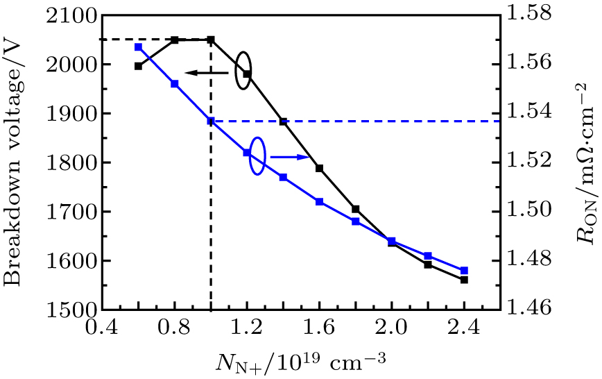
 | Fig. 9. Plot of optimized VBK and RON versus NN+ with NN+ ranging from 6× 1018 cm−3 to 2.4× 1019 cm−3 and LGN taking optimized value. |
Figure
 | Fig. 10. Plot of optimized VBK and RON versus LGN with LGN ranging from 3 μm to 14 μm and NN+ bing 1× 1019 cm−3. |
Figure
Figure
Summarized in Table
| Table 2. Comparison of device characteristic between device in this paper and other reported GaN devices. . |
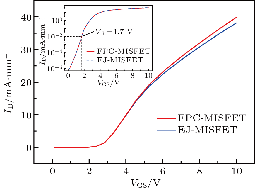
We investigated the behavior of the GaN MISFET structure with embedded pn junction which realizes the improvement of the device electric field distribution. It is shown that the breakdown voltage of the proposed EJ-MISFET reaches up to 2050 V. Compared with the FPC-MISFET, the EJ-MISFET provides 32.54% improvement in the breakdown voltage. The RON of the proposed EJ-MISFET is 15.37 Ω ⋅mm. The transfer characteristic keeps almost the same and the VTH values of two structures are both 1.7 V. The optimized device with LGN = 13 μm exhibits a high power BFOM of 2.734 GW⋅cm−2, VBK of 2050 V, and an RON of 15.37 Ω ⋅mm. Compared with that of the FPC-MISFET, the Baliga’s figure of merit of the EJ-MISFET is enhanced by 71.3%.
| [1] | |
| [2] | |
| [3] | |
| [4] | |
| [5] | |
| [6] | |
| [7] | |
| [8] | |
| [9] | |
| [10] | |
| [11] | |
| [12] | |
| [13] | |
| [14] | |
| [15] | |
| [16] | |
| [17] | |
| [18] | |
| [19] | |
| [20] | |
| [21] | |
| [22] | |
| [23] | |
| [24] | |
| [25] | |
| [26] | |
| [27] | |
| [28] | |
| [29] | |
| [30] | |
| [31] | |
| [32] | |
| [33] | |
| [34] | |
| [35] | |
| [36] | |
| [37] | |
| [38] | |
| [39] | |
| [40] |


