High-mobility SiC MOSFET with low density of interface traps using high pressure microwave plasma oxidation
Liu Xin-Yu1, 2, ‡, Hao Ji-Long1, 2, You Nan-Nan1, 2, Bai Yun1, 2, Tang Yi-Dan1, 2, Yang Cheng-Yue1, 2, Wang Sheng-Kai1, 2, §
Institute of Microelectronics, Chinese Academy of Sciences, Beijing 100029, China
University of Chinese Academy of Sciences, Beijing 100049, China


† Corresponding author. E-mail: xyliu@ime.ac.cn wangshengkai@ime.ac.cn

Project supported in part by the National Key Research and Development Program of China (Grant No. 2016YFB0100601), the National Natural Science Foundation of China (Grant Nos. 61674169 and 61974159), and the Support from a Grant-In-Aid from the Youth Innovation Promotion Association of the Chinese Academy of Sciences.

Abstract

The microwave plasma oxidation under the relatively high pressure (6 kPa) region is introduced into the fabrication process of SiO2/4H-SiC stack. By controlling the oxidation pressure, species, and temperature, the record low density of interface traps (∼ 4 × 1010 cm−2⋅eV−1@Ec − 0.2 eV) is demonstrated on SiO2/SiC stack formed by microwave plasma oxidation. And high quality SiO2 with very flat interface (0.27-nm root-mean-square roughness) is obtained. High performance SiC metal–oxide–semiconductor field-effect transistors (MOSFETs) with peak field effect mobility of 44 cm−2 ⋅eV−1 is realized without additional treatment. These results show the potential of a high-pressure plasma oxidation step for improving the channel mobility in SiC MOSFETs.

1. Introduction

SiC metal–oxide–semiconductor field-effect transistors (MOSFETs) are the promising devices for applications in areas where high power, high temperature, and high speeds are desired.[1] However, one of the technological concerns that affect the behavior of 4H-SiC MOSFETs is the low inversion channel mobility. In general, the channel mobility less than 10 cm2⋅V−1⋅s−1 is typically obtained by using thermally grown SiO2 layers as gate oxide.[2] This is about two orders of magnitude below the bulk mobility of 4H-SiC, the polytype most commonly investigated for power electronics applications, due to the high density of interface traps (Dit), in the order of 1013 eV−1⋅cm−2, near the conduction band edge. It is attributed to the existence of different types of charge traps either in gate oxide or at the SiO2/SiC interface, such as the dangling bonds, carbon clusters, and near interface traps.[3] Various channel engineering processes have been proposed to address these issues beyond nitrogen-monoxide (NO) annealing,[49] the process that is currently most widely used, but rarely leads to mobility above 40 cm2⋅V−1⋅s−1, especially with a heavy p-type doping concentration (> 1017 cm−3).[1012] This doping level is typical for power double implanted MOSFETs (DMOSFETs).

Plasma oxidation, utilizing a highly activated oxygen plasma, is one of the low temperature techniques used to grow dielectric films on semiconductor surfaces. The study of SiC oxidation by plasma began around 1997 and Lucovsky et al. reported that SiC can be oxidized by remote plasma-assisted oxidation.[13] Recently, Kim et al. investigated that interface traps generation in the SiO2 oxide is more suppressed in the high-power plasma oxidation process than in the thermal oxidation process.[14,15] Early studies preliminarily revealed the equipment principle of plasma oxidation, mechanism of plasma oxidation, and characteristics of plasma oxide.[1618] However, the plasma oxidation has not been reported for the fabrication of SiC MOSFET.

In the present article, for the first time, high-pressure microwave plasma oxidation process has been introduced for SiC MOSFETs fabrication. We have systematically studied the material and electrical characteristics of the plasma oxide layer. And the MOSFETs with a heavy p-type doping concentration (∼ 1017 cm−3) were fabricated and the field effect mobility was extracted. The high-pressure plasma SiO2/4H-SiC stack presents a significant improvement of interface properties over those grown by other oxidation methods.

2. Experiment and measurement
2.1. Plasma oxidation facility

A schematic diagram of the microwave oxidation equipment used in our work is shown in Fig. 1(a). The primary components of the apparatus are a microwave generator (2.45 GHz) capable of delivering up to 2000 W, water-cooled waveguides, a reactor cavity (4 cm in diameter and 15 cm in length). In addition, the surface temperature of SiC was detected from the top infrared thermometer. The pure (7N) oxygen was used as the reactant gas throughout this work. From the observation window, a plasma hemisphere was observed that touched the surface of SiC and was located at the center of the chamber, as shown in the inset.

Fig. 1. (a) Schematic diagram of microwave plasma oxidation equipment. 2.45-GHz microwave generated by a magnetron is guided through the waveguide to the quartz discharge tube filled with pure oxygen gas. A plasma hemisphere with a diameter of 2.5 cm was well confined and located at the center of the chamber, as depicted in the inset. (b) SiC surface temperature as a function of O2 pressure and plasma power. (c) OES of plasma under various chamber pressures by fixing the power at 500 W.
2.2. Device fabrication

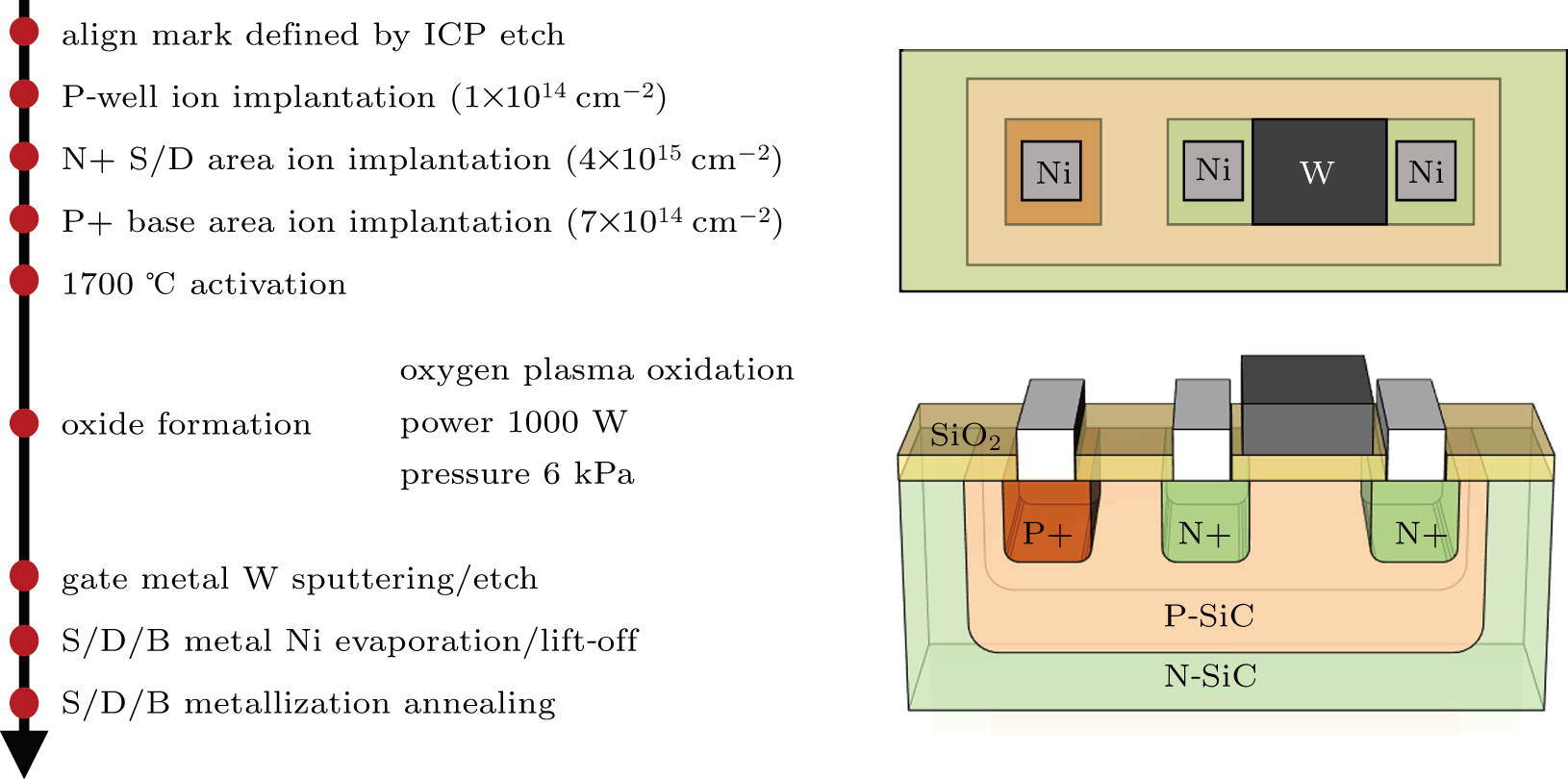
All devices were fabricated on the N-type epitaxial layer (dopant density ≈ 1 × 1016 cm−3) deposited on the (0001) Si-face of 4H-SiC wafers. The fabrication process of metal–oxide–semiconductor (MOS) capacitors is as follows. 4H-SiC wafers were precleaned by using deionized water, acetone, and HF aqueous solution. Then the plasma oxide was grown in the microwave chamber at room temperature and pressure of 6 kPa under a flow of purity (7N) O2 gas and an optimized microwave power of 1000 W.[19] Al electrodes were deposited to form gate (diameter is about 200 μm for capacitance–voltage (CV) measurement; thickness ≈ 400 nm) and backside Ohmic contacts. The fabrication process of MOSFET is shown in Fig. 2. To obtain the surface aluminum (Al) concentrations of 1 × 1017 cm−3, box-shaped, p-type wells, and p+ contact regions (∼ 1 × 1020 cm−3) were all fabricated by multiple Al-implantations into the epitaxial layer at 500 °C. Source and drain regions (∼ 1 × 1020 cm−3) were implanted with nitrogen at room temperature. Then the SiC surface was capped with a graphite layer, and the implants were activated at 1700 °C. After a sacrificial oxidation, the gate oxide was grown by using 6-kPa plasma oxidation with the microwave power of 1000 W. Next, a 600-nm layer of tungsten was deposited and patterned for the gate metal and an 80-nm-thick nickel layer was deposited over the source and drain for Ohmic contacts. The Ohmic contacts were alloyed at 970 °C for 2 min. The channel width of the MOSFETs is 100 μm and the length is 50 μm.

Fig. 2. Fabrication procedure and device structure of the SiC n-MOSFETs with SiO2 gate stacks. Note that the figure shows the ion implantation dose.
2.3. Material characterization

The direct characterization of the SiO2/4H-SiC interface was measured by the transmission electron microscope (TEM). The high resolution TEM images were obtained using a field-emission gun at an acceleration voltage of 200 keV. The chemical bonding states of the SiO2 films grown on the 4H-SiC substrates were examined via high-resolution x-ray photoelectron spectroscopy (XPS); a monochromatic Al x-ray source ( = 1486.7 eV) with a pass energy of 55 eV and a resolution energy of 0.1 eV was used. Si-2p, C-1s, O-1s, and N-1s spectra were recorded. Binding energies (BE) was corrected for charging effects assuming the BE of the contaminant C-1s peak as lying at 284.6 eV. The interface roughness of the samples was measured via the atomic force microscopy (AFM). Before testing, the oxide of all samples was completely removed by using buffer oxide etch (BOE) solution for 60 minutes. Then the morphology of SiO2/4H-SiC interface was examined with testing area of 1 μm × 1 μm. The AFM (XE-200, Park Systems) was used for the surface measurement. Park Systems AFM XEI software programming was used to evaluate the root-mean-square roughness (RMS roughness).

2.4. Electrical characterization

In order to further evaluate the quality of the oxide and the interface formed by the plasma oxidation, the MOS capacitances and MOSFETs were analyzed by the electrical measurements. The capacitance–voltage (CV) measurement was performed with an Agilent E4990A LCR meter. The density of interface traps (Dit) values were estimated by the conductance method at various temperatures.[20,21] The MOSFET DC characteristics were measured with an Agilent B1500 A semiconductor parameter analyzer. Drain current (Id) as a function of gate voltage (Vg) (IdVg) for the MOSFET was measured. The data were collected with the drain voltage (Vd) held at a constant 50-mV bias. And the Id as a function of Vd (IdVd) was also measured with the Vg ranging from 2 V to 8 V.

3. Results and discussion
3.1. SiO2 grown by microwave plasma oxidation

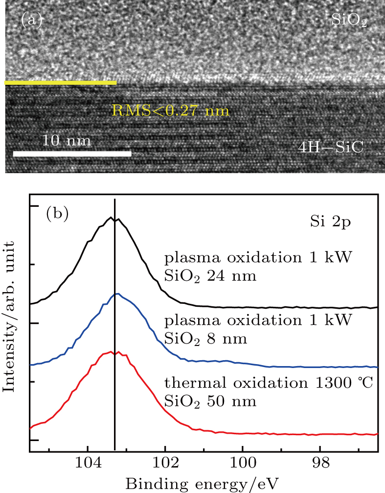
Figure 1 (b) shows the SiC surface temperature by varying O2 pressure and plasma power. The surface temperature ranging from 750 °C to 900 °C is found to be linearly proportional to the chamber O2 pressure by fixing the power at 1000 W. Moreover, it is also known that the temperature can be further adjusted by changing the microwave power. Concerning the origin of the in situ self-heating process during oxidation, heat accumulation related to O2 molecular emission may be the main reason. As the O2 pressure increased, optical emission at around 400–700 nm significantly grows, as depicted in Fig. 1(c). The oxygen plasma is confirmed to be dominated by excited atomic O plasma (O*), according to the feature of 777 nm, 844 nm, and 485 nm.[22] To evaluate the quality of SiO2/SiC, two SiO2 samples with thickness of 8 nm and 24 nm were prepared under an optimized condition (chamber pressure=6 kPa, power=1000 W). As shown in Fig. 3(a), sharp and very flat interface with RMS roughness value less than 0.27 nm is obtained after oxidation, which is comparable to the initial surface roughness of the as-cleaned SiC wafer and hardly be obtained by conventional thermal oxidation. This result suggests almost no accumulation of residual carbon at the interface. Figure 3(b) shows the XPS spectra of Si 2p for the 8-nm and 24-nm SiO2/SiC stacks, 1300 °C thermally grown SiO2/SiC stack is also listed out for comparisons. For the 8-nm SiO2 sample, a small hump is observed in the range of 100–101 eV,[23] which is assigned to SiC substrate. Thus, the Si 2p of the 8-nm SiO2 must include the signal from the interfacial transition region. While for the 24-nm SiO2 case, Si-2p signal should come from the surface region where almost no contribution of interfacial transition region is included. Since signal related to SiO2 in the three spectra are almost the same, it strongly indicates that high quality SiO2 comparable to thermally grown SiO2 with almost no interfacial transition region is obtained, this result is consistent with our previous electron energy loss spectroscopy results.[19] It should be noted that there is no N-1s signal, eliminating the existence of N contamination during the plasma oxidation process.

Fig. 3. (a) Cross-sectional TEM image of the SiO2/SiC stack. (b) Comparison of XPS Si-2p spectra between microwave plasma oxidized SiO2 and 1300 °C thermally grown SiO2.
3.2. SiC MOS capacitor characterization

Figure 4 (a) shows the multi-frequency bidirectional CV curves of the MOS capacitors fabricated by plasma oxidation with pressure of 6 kPa and power of 1000 W measured at 100 K and 300 K and a 1300-°C thermal oxidized sample (the thickness of SiO2 is 50 nm) with NO annealing as a reference. The thickness value of plasma oxide, 25.7 nm, is evaluated by the oxide capacitance for the unit area (Cox). Cox is determined by the extrapolation of high frequency capacitance in accumulation region, as shown in Fig. 4(b). Compared with NO annealed thermal oxidized sample, nearly frequency dispersion free CV curves with hysteresis less than 50 mV are observed in 1000-W case, especially at 100 K, strongly indicating that high quality SiO2/SiC stack with low Dit can be achieved through microwave plasma oxidation.

Fig. 4. (a) Multi-frequency bidirectional CV curves of the MOS capacitors fabricated by plasma oxidation with pressure of 6 kPa and power of 1000 W and 1300-°C thermal oxidation with NO annealing measured at 100 K and 300 K. (b) The Cox of 1000-W plasma oxidized MOS capacitor is determined by the extrapolation of high frequency capacitance in accumulation region.

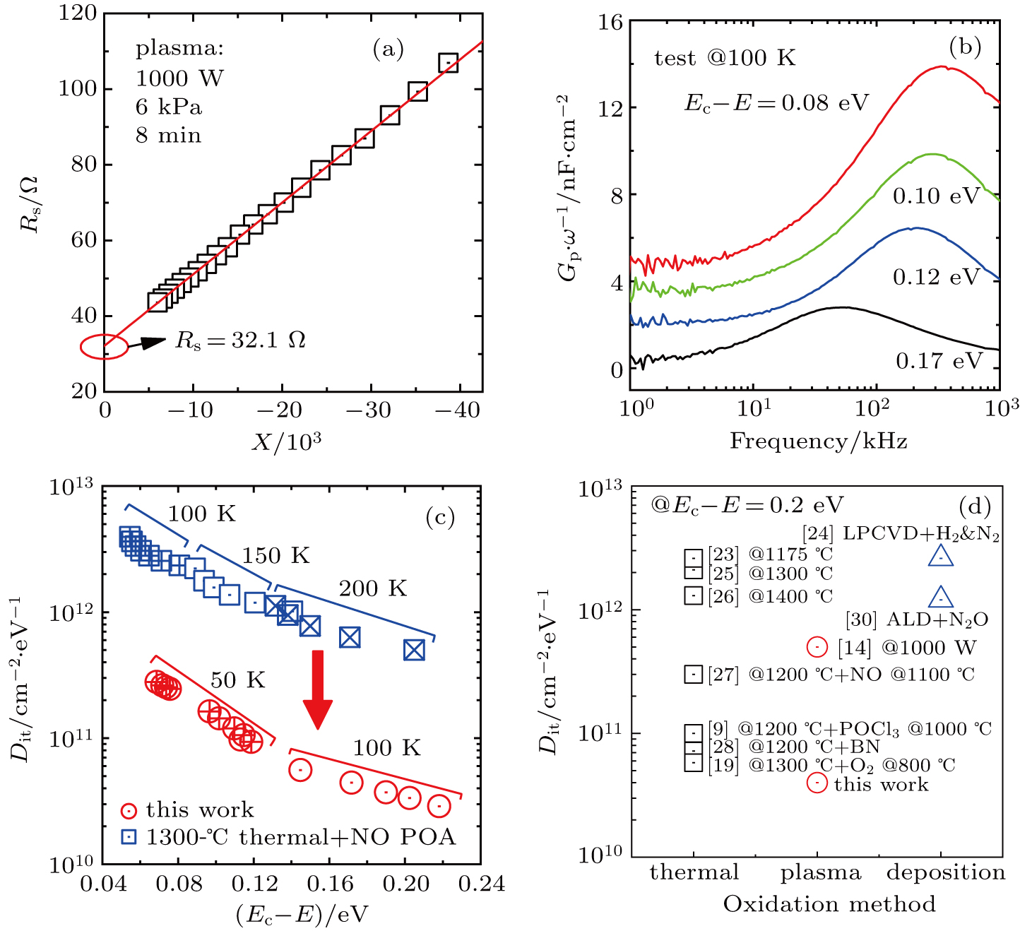
The Dit values were determined via calculations by using a combination of forward bias capacitance–frequency (Cf) and conductance–frequency (Gf) measurements to obtain the parallel conductance (Gp), as shown in Fig. 5(b), while the energy levels of the defect states were determined from frequency measurements. The Dit is approximated as the following relationship:[20]

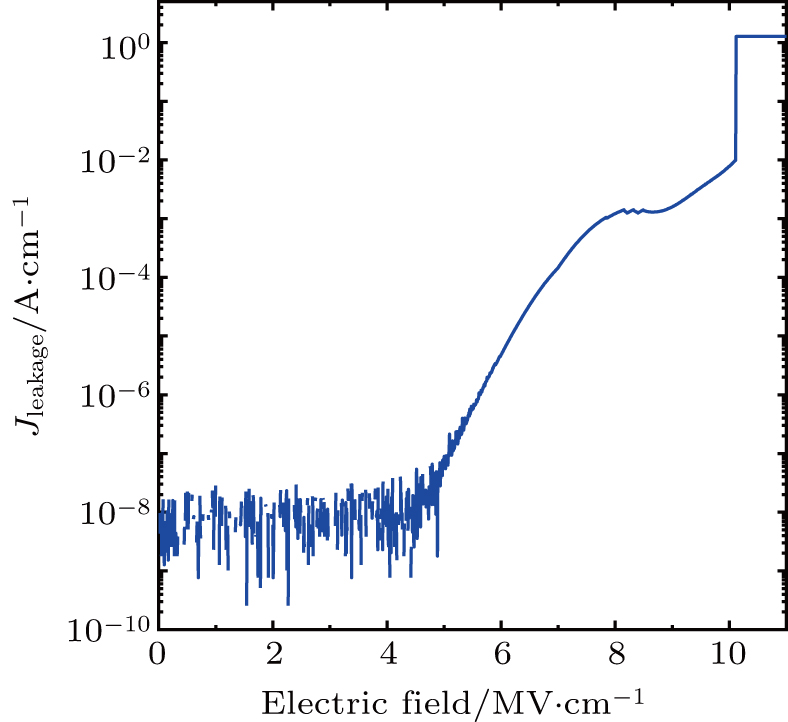
where A is the area of the electrode and q is the elemental charge. Before applying the conductance method, series resistance (Rs) was determined by the extrapolation of high frequency limit of the real part of impedance measured in accumulation region, as shown in Fig. 5(a).[21] Then, Rs was removed from the measured impedance. The measurements were done at the temperature from 50 K to 200 K to extend the energy range of the characterization toward the conduction band edge of SiC. As a result, the value of Dit for 1000-W plasma-oxidized sample is lower than 1011 cm−2⋅eV−1 at the energy level range from 0.1 eV to 0.2 eV below the 4H-SiC conduction band edge, as shown in Fig. 5(c). And the Dit value is one order of magnitude lower than the NO annealed thermal oxidized sample, nearly catching up with the SiO2/Si level. As shown in Fig. 5(d), to our knowledge, this work is the record low published Dit in SiO2/SiC system,[9,14,2431] confirming the effectiveness of high-pressure oxidation in forming high quality SiO2/SiC stack. And it is found that the breakdown field for the 1000-W sample could reach 10 mV/cm, as shown in Fig. 6, which is comparable to the breakdown field of the high temperature thermal oxidized sample. It proves that the plasma oxidation method has a great potential in both maintaining high oxide reliability and low Dit.

Fig. 5. (a) The Rs determined by the extrapolation of high frequency limit of the real part of impedance measured in accumulation region. (b) Frequency dependence of Gp/ω measured at 100 K. (c) The Dit as a function of energy level below the conduction band, estimated from the peak values of Gp/ω measured at the temperature from 50 K to 200 K and the NO annealed thermal oxidized sample is the reference group. (d) The Dit of the sample oxidized by plasma oxidation compared with the other oxidation method in previous reports, as a function of energy level of 0.2 eV below the 4H-SiC conduction band edge.
Fig. 6. The typical JE characteristics of MOS capacitors formed by 1000 W plasma oxidation.
3.3. SiC MOSFET characterization

Figure 7 (a) shows the raw transfer characteristics of the MOSFETs with channel length of 50 μm. On/off ratio of over 107 with the minimal subthreshold swing (SS) of ∼ 110 mV/dec is obtained. Series resistance of 390 Ω is extracted from the intercept by plotting the Ron against channel length. The output characteristics of the SiC MOSFET with channel width (W) = 100 μm, length (L) = 50 μm are shown in Fig. 7 (b). From transfer characteristic, we calculate field-effect channel mobility (μFE) through the relationship:[32]

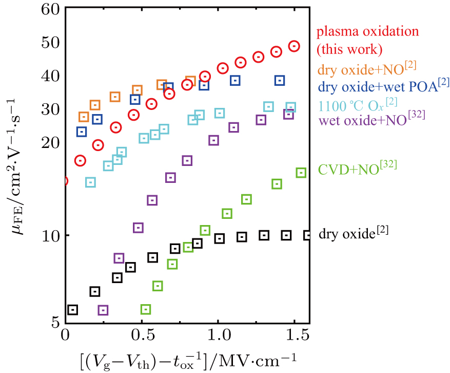
Figure 8 shows the μFE as a function of the normalized electric field (VgVth/tox) in 4H-SiC MOSFETs with different gate oxides subjected to plasma oxidation, thermal oxidation, nitridations (NO) or wet annealing treatments.[2,33] The peak μFE of 44 cm2⋅V−1⋅s−1 can be obtained for plasma oxidation. For inversion type MOSFETs, although higher mobility has been reported by doping P, B, Ba into the SiO2 network,[33] most of these approaches are still far to be used for real applications, because they suffer from threshold voltage instability issues due to the fragile network. Moreover, for most of the previous reports, the p-body doping densities are lower than 1016 cm−3. Kimoto et al. have reported that the sub-bands are shifted upward with increasing the p-body doping, leading to a stronger quantum confinement effect.[34] Thus, the energy levels of Dit of the NO annealed sample exhibits a sharp increase toward (and likely inside) the conduction band edge in SiC. Therefore, the mobility of NO annealed sample on a more heavily doped p-body, affected by a higher Dit located at higher energy levels, drops significantly in heavily-doped MOSFETs. The peak mobility of the NO sample dropped to lower than 30 cm2⋅V−1⋅s−1 with a heavy p-type doping concentration (∼ 1017 cm−3).[11,12,35] Plasma-oxidized SiO2 exhibits a relatively high field effect mobility with a heavy p-type doping concentration (∼ 1017 cm−3) compared with other oxidation processes. By considering the low Dit, flat interface, and high mobility, it is clear that high quality SiO2/SiC stack can be obtained by using plasma oxidation method.

Fig. 7. (a) Transfer characteristics of SiC MOSFETs with channel lengths of 50 μm fabricated by plasma oxidation. (b) Output characteristics of SiC MOSFET with channel lengths of 50 μm fabricated by plasma oxidation.
Fig. 8. Field effect mobility (μFE) as a function of the normalized electric field in 4H-SiC MOSFETs with different gate oxides subjected to plasma oxidation, thermal oxidation, nitridations (NO) or wet annealing treatments.
4. Conclusion and perspectives

A high-pressure plasma oxidation process has been demonstrated on 4H-SiC yielding a lower Dit than numerous literature reports of thermal oxides. Field effect mobilities of ∼ 44 cm2⋅V−1⋅s−1 have been extracted from lateral channel MOSFETs with a heavy p-type doping concentration (∼ 1017 cm−3). This is higher than other reports of mobility in 4H-SiC MOSFETs with thermally grown oxides. The enhanced mobility is most likely due to a reduction in trapped charge. The findings in this work demonstrate that a high-pressure plasma oxidation step may be a promising process for improving the channel mobility in SiC MOSFETs.

Reference
[1] Siddiqui A Elgabra H Singh S 2016 IEEE Trans. Dev. Mater. Reliab. 16 419
[2] Hirai H Kita K 2018 Appl. Phys. Lett. 113 172103
[3] Peng Z Y Wang S K Bai Y Tang Y D Chen X M Li C Z Liu K A Liu X Y 2018 J. Appl. Phys. 123 135302
[4] Li H F Dimitrijev S Harrison H B Sweatman D 1997 Appl. Phys. Lett. 70 2028
[5] Jamet P Dimitrijev S 2001 Appl. Phys. Lett. 79 323
[6] Chakraborty S Lai P T Kwok P C K 2002 Microelectron. Reliab. 42 455
[7] Xu J P Lai P T Chan C L 2003 Solid-State Electron. 47 1397
[8] Kosugi R Fukuda K 2004 Mater. Sci. Forum 457 1345
[9] Okamoto D Yano H Hirata K Hatayama T Fuyuki T 2010 IEEE Electron Dev. Lett. 31 710
[10] Chung G Y Tin C C Williams J R McDonald K Chanana R K Weller R A Pantelides S T Feldman L C Holland O W Das M K Palmour J W 2001 IEEE Electron Dev. Lett. 22 176
[11] Tilak V Matocha K Dunne G 2007 IEEE Trans. Electron Dev. 54 2823
[12] Noguchi M Iwamatsu T Amishiro H Watanabe H Kita K Yamakawa S 2017 IEEE International Electron Devices Meeting (Iedm), 2–6 December, 2017 San Francisco, CA, USA 9.3.1 9.3.4 10.1109/IEDM.2017.8268358
[13] Gölz A Lucovsky G Koh K Wolfe D Niimi H Kurz H 1997 Microelectron. Eng. 36 73
[14] Kim D K Jeong K S Kang Y S Kang H K Cho S W Kim S O Suh D Kim S Cho M H 2016 Sci. Rep. 6 34945
[15] Kim D K Cho M H 2017 Appl. Sci. Converg. Technol. 26 133
[16] Masataka S Hisanori S Tomonori N Sachiko Y 2002 Jpn. J. Appl. Phys. 41 L233
[17] Satoh M Shimada H Nakamura T Nagamoto N Yanagihara S 2002 Mater. Sci. Forum 389 1105
[18] Hanafusa H Ishimaru R Higashi S 2017 Jpn. J. Appl. Phys. 56 040304
[19] Liu X Y Hao J L You N N Bai Y Wang S K 2019 AIP Adv. 9 125150
[20] Okamoto D Yano H Hatayama T Fuyuki T 2010 Appl. Phys. Lett. 96 203508
[21] Nicollian E H Brews J R Nicollian E H 1982 MOS Physics Technology Chichester John Wiley and Sons 212 221
[22] Dzioba S Este G Naguib H M 1982 J. Electrochem. Soc. 129 2537
[23] Watanabe H Hosoi T Kirino T Kagei Y Uenishi Y Chanthaphan A Yoshigoe A Teraoka Y Shimura T 2011 Appl. Phys. Lett. 99 021907
[24] Chung G Y Williams J R Isaacs-Smith T Ren F McDonald K Feldman L C 2002 Appl. Phys. Lett. 81 4266
[25] Rozen J Nagano M Tsuchida H 2013 J. Mater. Res. 28 28
[26] Kobayashi T Suda J Kimoto T 2017 AIP Adv. 7 045008
[27] Sometani M Nagai D Katsu Y Hosoi T Shimura T Takei M Yonezawa Y Watanabe H 2017 Jpn. J. Appl. Phys. 56 04cr04
[28] Jamet P Dimitrijev S Tanner P 2001 J. Appl. Phys. 90 5058
[29] Okamoto D Sometani M Harada S Kosugi R Yonezawa Y Yano H 2014 IEEE Electron Dev. Lett. 35 1176
[30] Kikuchi R H Kita K 2014 Appl. Phys. Lett. 105 032106
[31] Yang X Y Lee B Misra V 2016 IEEE Trans. Electron Dev. 63 2826
[32] Lundstrom M Guo J 2006 Nanoscale transistors: device physics, modeling and simulation New York Springer Science and Business Media 39 80
[33] Roccaforte F Fiorenza P Greco G Nigro R L Giannazzo F Iucolano F Saggio M 2018 Microelectron Eng. 187 66
[34] Kimoto T Niwa H Kajil N Kobayashi T Zhao Y Mori S Aketa M 2017 IEEE International Electron Devices Meeting (Iedm), 2–6 December, 2017 San Francisco, CA, USA 9.5.1 9.5.4 10.1109/IEDM.2017.8268360
[35] Ohashi T Nakabayashi Y Iijima R 2018 IEEE Trans. Electron Dev. 65 2707