Organic field-effect transistor floating-gate memory using polysilicon as charge trapping layer
Zhang Wen-Ting1, 2, Wang Fen-Xia1, Li Yu-Miao1, Guo Xiao-Xing1, Yang Jian-Hong1, †
Institute of Microelectronics, Lanzhou University, Lanzhou 730000, China
School of Electronic and Information Engineering, Lanzhou Jiaotong University, Lanzhou 730070, China


† Corresponding author. E-mail: yangjh@lzu.edu.cn

Abstract

In this study, we present an organic field-effect transistor floating-gate memory using polysilicon (poly-Si) as a charge trapping layer. The memory device is fabricated on a N+–Si/SiO2 substrate. Poly-Si, polymethylmethacrylate, and pentacene are used as a floating-gate layer, tunneling layer, and active layer, respectively. The device shows bidirectional storage characteristics under the action of programming/erasing (P/E) operation due to the supplied electrons and holes in the channel and the bidirectional charge trapping characteristic of the poly-Si floating-gate. The carrier mobility and switching current ratio (Ion/Ioff ratio) of the device with a tunneling layer thickness of 85 nm are and 102, respectively. A large memory window of 9.28 V can be obtained under a P/E voltage of ±60 V.

1. Introduction

Organic memory devices have attracted widespread attention in recent years due to their low cost, light weight, solution processability, and mechanical flexibility characteristics.[13] The different material systems and working mechanisms used in organic memory devices can be classified into three different configurations, namely, capacitor-type,[4] resistor-type,[5] and transistor-type memories.[6] Among these memory devices, transistor-type organic field-effect transistor memory (OFETM) devices have many advantages, such as single-transistor realization,[7] nondestructive readout,[8] multi-bit storage,[9,10] and compatibility with CMOS technology. OFETM devices have a structure similar to that of an organic field-effect transistor (OFET), except for a supplementary charge trapping layer that is inserted into the gate dielectric.[11] Considerable efforts have been made to enhance the performance of OFET floating-gate memory (OFET-FGM) devices. One effective method is to use different conductive or semi-conductive nanoparticles or nanofilms as floating-gates. For example, Au, Ag, Cu, and Pt metal nanoparticles are used as nano-floating-gates to increase the memory window and retention time because trap levels and trap sites can be precisely controlled by the nanoparticles’ species, size, and density.[1215] Carbon-based nanoparticles include graphene quantum dots,[16] which are a promising alternative to traditional semiconductors due to their easy solution processing techniques and excellent physical and chemical properties; reduced graphene oxide;[17] single-walled carbon nanotubes; and[2] C60.[18] Other floating-gate materials include transition metal dichalcogenides (MoS2),[19] electret materials,[20] and hybrid nanostructures.[21,22] However, the preparation of rare metal nanoparticles is expensive and this process is prone to agglomeration. Two-dimensional (2D) materials are difficult to peel and can easily be contaminated during transfer. As a charge trapping material, polysilicon (poly-Si) has widely been used in inorganic memory devices.[23] However, its application in organic memory has rarely been reported. In the current study, we developed and characterized a nanostructured OFET-FGM device with poly-Si as a floating-gate. The relevant results show that poly-Si exhibits excellent charge capture characteristics in organic memory devices.

The materials and surface morphology of the tunneling layer have a huge influence on the performance of OFET-FGM. The use of different organic materials as a tunneling layer can effectively improve the programming/erasing (P/E) voltage, memory window, and storage switching current ratio of the devices.[24,25] In this experiment, polymethylmethacrylate (PMMA) is used as the tunneling layer of OFET-FGM, the performance of the device is improved by optimizing the tunneling layer thickness, and the typical thickness of the OFET-FGM device is 85 nm.

2. Experiment

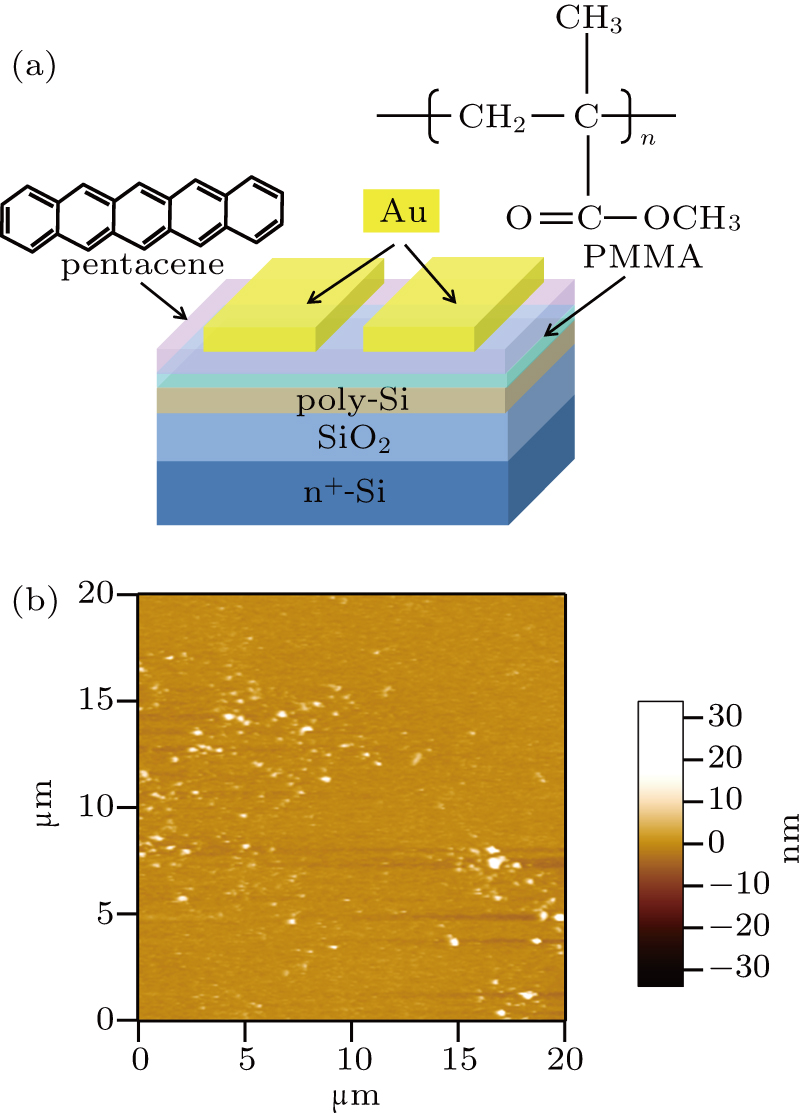
The schematic stereoscopic structure of the OFET-FGM device is shown in Fig. 1(a). The devices were fabricated on heavily doped Si substrates with 300-nm-thick SiO2 on top to form the control gate and control dielectric. Then, 50-nm-thick poly-Si was deposited onto the SiO2 surface through low-pressure chemical vapor deposition as the floating-gate layer. Figure 1(b) is an AFM image of poly-Si film on the SiO2 surface, and the root mean square (RMS) surface roughness is 1.580 nm. Then, PMMA was dissolved in toluene at 7 mg/mL and the resulting solution was spin-coated on top of the poly-Si, followed by annealing in a vacuum-drying oven at 100 °C for 2 h to form a tunneling layer. The thickness of the PMMA tunneling layer was measured to be 85 nm by using an ellipsometer. Subsequently, 50-nm-thick pentacene was deposited onto the PMMA surface through vacuum deposition in a high-vacuum system at a pressure of (1 bar = 105 Pa), where the deposition rate was approximately 0.15 Å/s, and the substrates were kept at room temperature. Finally, 70-nm-thick Au was deposited on the pentacene through thermal evaporation on a shadow mask to fabricate the drain and source electrodes, where the working pressure was and the deposition rate was kept at 0.3 Å/s. For comparison, a control sample without a poly-Si charge trapping layer was simultaneously prepared following the same process. Electrical characterization of the devices was performed with a Keithley 4200 semiconductor characterization system under the atmospheric environment and room temperature.

Fig. 1. (a) Schematic diagram of device structure and (b) AFM image of poly-Si film on SiO2 surface.
3. Results and discussion
3.1. Output and transfer characteristics of OFET-FGM device

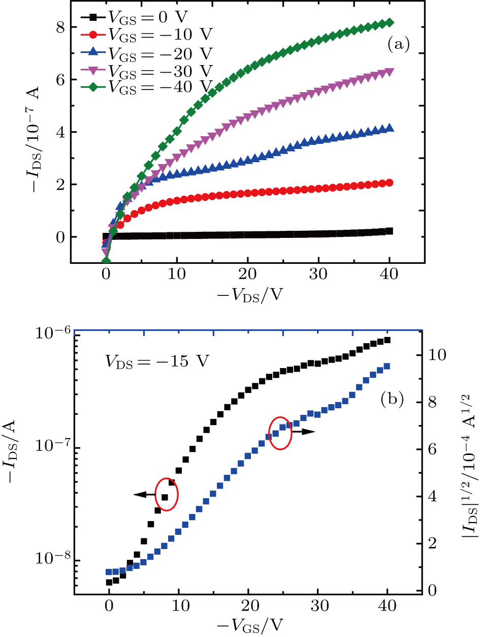
The output characteristics of the OFET-FGM are shown in Fig. 2(a), which shows the characteristics of an excellent p-channel field-effect transistor in a hole accumulation mode under a drain–source voltage (VDS) ranging from 0 V to −40 V and a gate–source voltage (VGS) from 0 V to −40 V in steps of −10 V. Figure 2(b) shows the initial transfer characteristics of the device. The field-effect mobility (μ) and threshold voltage (VT) of the device can be calculated by using the following formula: where Ci is the insulator capacitance per unit area, and the channel length (L) and width (W) of these devices are and m, respectively. In this multilayer thin-film OFET-FGM, two different insulating layers are found, where the first layer is a 300-nm-thick SiO2 layer (gate insulator layer), and the second layer is an 85-nm-thick PMMA layer (tunneling layer). The capacitance (Ci) of the devices can be calculated by using the equation where dg and dt are the thickness of the gate insulator layer (SiO2) and tunneling layer (PMMA), and and are the dielectric constant of the gate insulator and tunneling layers, respectively. The calculated Ci of the OFET-FGM is 8.961 nF/cm2. The calculated value of μ for the OFET-FGM is . The VT and Ion/Ioff ratio of the OFET-FGM are −0.98 V and 102, respectively. The control sample (without a poly-Si layer) possesses analogous electrical characteristics to the OFET-FGM. The characteristic parameters (μ, VT, and Ion/Ioff ratio) of the control sample are , −11.84 V, and 104, respectively.

Fig. 2. (a) Output characteristics and (b) transfer characteristics of OFET-FGM.
3.2. Electrical memory characteristics of OFET-FGM device

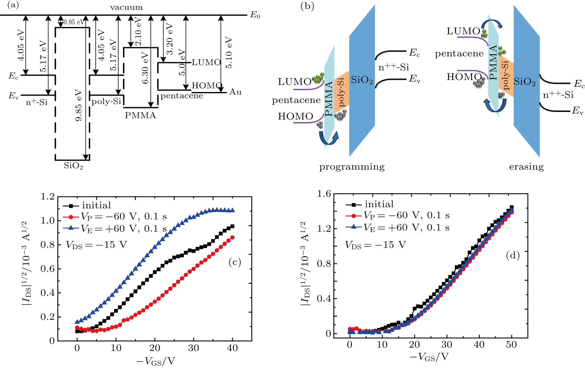
The energy level of the present OFET-FGM is shown in Fig. 3(a), where E is the vacuum energy level, and the lowest unoccupied molecular orbital level (LUMO), and the highest occupied molecular orbital level (HOMO) of pentacene are −3.2 eV and −5.0 eV, respectively. As shown in Fig. 3(b), holes from the channel are injected and trapped into the floating-gate when a negative pulse voltage is applied to the gate electrode. The holes captured by the poly-Si floating-gate generate an internal electric field, which is in the opposite direction to the applied negative gate voltage. Therefore, a greater negative voltage is needed to open the OFET-FGM, which leads to a negative direction shift of VT. This process is called the programming (P) operation. The erasing (E) operation is the opposite process to P as shown in Fig. 3(b). Considering that most organic small-molecule field-effect materials show single-polar characteristics, the transfer curve of the memory device returns to the initial state after the E operation.[11] However, some molecules can exhibit bipolar transmission characteristics under the action of different dielectric layer modifications and different device structures.[6] As shown in Fig. 3(c), the transfer curve of the OFET-FGM prepared in this experiment shifts toward the positive direction of the initial transfer curve. This condition indicates that pentacene exhibits bipolar transmission characteristics in this experiment. Holes trapped in the floating-gate are extracted back to the active layer when a positive pulse voltage is applied to the gate. Then, the minority electrons in the active layer are injected into the floating-gate under the action of positive gate pulse voltage. The electrons captured by the poly-Si floating-gate form an internal electric field in the same direction of the applied negative gate voltage, thus leading to a positive drift of VT. Figure 3(c) shows the transfer characteristics of the OFET-FGM at the initial, programming, and erasing states. The programming voltage (VP) and erasing voltage (VE) are −60 V for 0.1 s and +60 V for 0.1 s, respectively. In addition, VDS is kept at 0 V in this P/E operation. The initial, programmed, and erased VT are −0.98 V, −6.87 V, and 2.41 V, respectively. A 9.28 V memory window ( ) is obtained. The transfer curves of the control sample (without a poly-Si floating-gate) are shown in Fig. 3(d). The insignificant drift of the threshold voltage indicates that charges are trapped in the poly-Si floating-gate layer.

Fig. 3. (a) Energy level diagram of OFET-FGM without applying voltage. (b) Energy band diagrams of OFET-FGM during P/E operation. (c) Memory window of OFET-FGM, VP/E = ±60 V, 0.1 s. (d) Memory window of control sample, VP/E = ±60 V, 0.1 s.

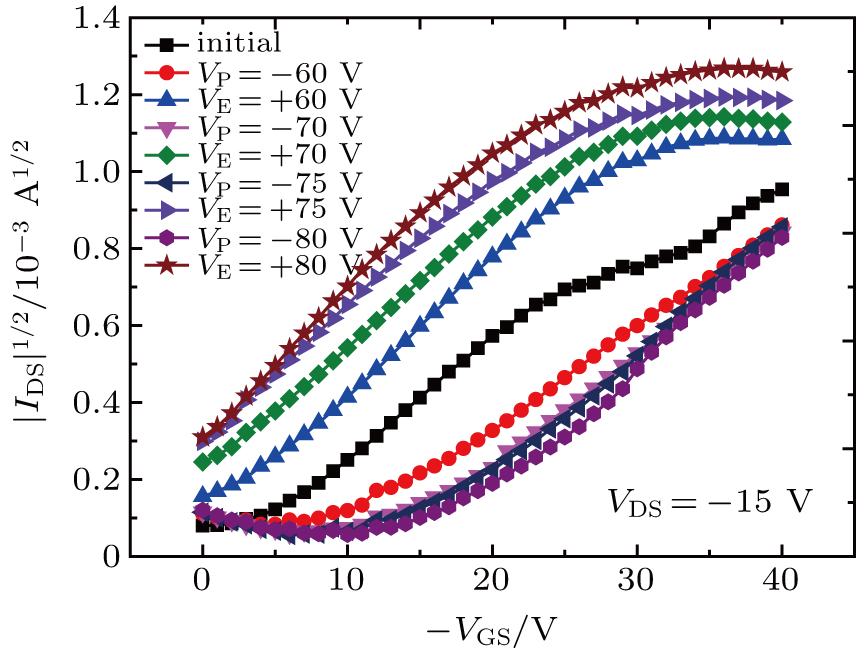
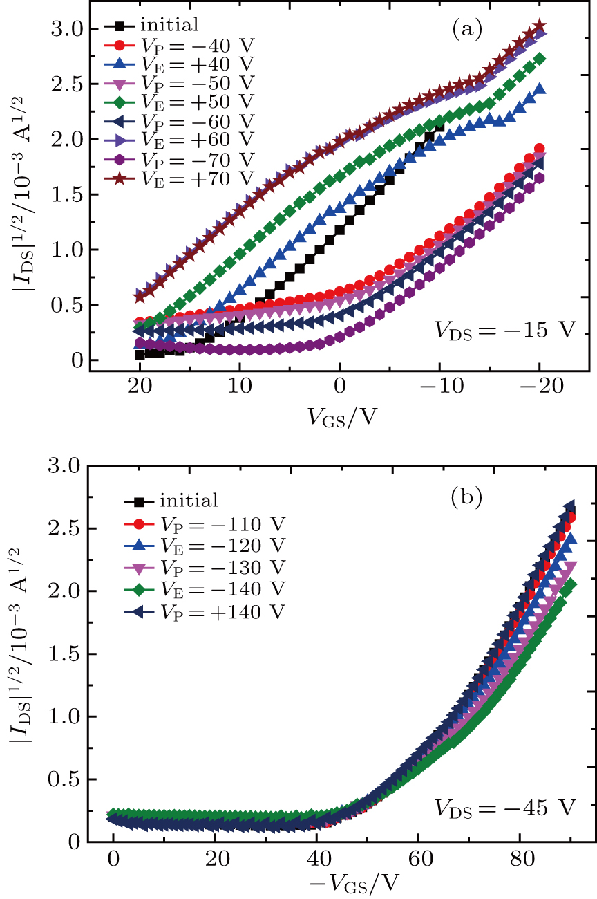
Figure 4 shows the transfer curves of the OFET-FGM device in the initial state and in a series of P/E operations under various VP/VE voltages at 0.1 s. The memory windows of the OFET-FGM increase with the increase of P/E voltage. Three main charge exchange mechanisms, namely, a hot-carrier injection mechanism, direct tunneling mechanism, and Fowler–Nordheim (FN) tunneling mechanism, are found between the active layer and floating-gate layer.[26] In our OFET-FGM, one of the charge exchange mechanisms between the active layer and floating-gate layer is the FN tunneling mechanism, which is attributed to the low field-effect mobility ( and thick tunneling layer (85 nm). The threshold voltages after P/E operation are −9.90 V and 8.86 V, which are obtained by fitting the transfer characteristic curves of VP = −70 V for 0.1 s and VE = +70 V for 0.1 s, respectively.

Fig. 4. Memory windows of OFET-FGM at various VP/VE voltages for 0.1 s.

Compared with the initial transfer characteristic curve, the change ratio of VT to VE is higher than that of VT to VP. This finding indicates that the number of electrons injected into the floating-gate during E operation is larger than the number of holes during P operation. This condition indicates that E operations can more easily occur than P operations under certain conditions, and that this phenomenon can be reasonably explained by the hot-carrier injection mechanism. As shown in Fig. 3(a), first, the barrier height of the holes skipping the tunneling layer (1.3 eV) during P operation is slightly higher than the barrier height (1.13 eV) during E operation; second, during E operation, holes stored in the floating-gate are injected into the channel, and electrons originating between the organic semiconductor layer and charge tunneling layer are injected into the conducting band of the poly-Si floating-gate from the LUMO level of pentacene. The barrier height (1.1 eV) of the electrons injected from the LUMO level of pentacene into the conduction band of poly-Si is lower than that of the holes injected from the HOMO level of pentacene into the valence band of poly-Si (1.3 eV). Therefore, two charge exchange mechanisms, namely, the hot-carrier injection and FN tunneling mechanisms, exist in the present OFET-FGM. Further, when the absolute value of the P/E voltage is greater than 80 V, the memory window of the OFET-FGM remains constant with the increase of P/E voltage, the charge quantity stored in the floating-gate is saturated, and the corresponding storage window is approximately 25 V. This condition is consistent with the simulation results previously reported by our group.[27]

The tunneling layer thickness affects the P/E voltage and retention time of the memory. Figure 5(a) and 5(b) show the memory windows of the devices at PMMA/toluene solution concentrations of 5 mg/mL and 11 mg/mL. The corresponding PMMA films’ thicknesses measured by ellipsometry are 75 nm and 146 nm, respectively. Compared with that of the sample described in the previous section, a lower P/E voltage is required for the OFET-FGM with a tunneling layer thickness of 75 nm. A memory window of approximately 15 V can be obtained under a P/E voltage of ±40 V for 0.1 s. The maximum memory window of approximately 25 V is achieved with the increase of P/E voltage and when VP/E = ±70 V. However, the memory windows decrease dramatically for the sample with a tunneling layer thickness of 146 nm. The reason is that with the increase of the thickness of the tunneling layer, FN tunneling is unlikely to occur even under a high programming voltage. The drifts of the transfer characteristic curves of Fig. 5(b) can be attributed to the charge trapping effect of PMMA[28] and to interface defect traps between the PMMA/pentacene surfaces.

Fig. 5. Memory windows at PMMA/toluene solution concentrations of (a) 5 mg/mL and (b) 11 mg/mL.
3.3. Retention characteristics of OFET-FGM device

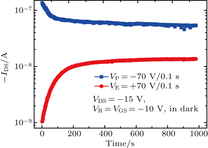
Figure 6 shows the retention characteristics of the sample with a PMMA/toluene solution concentration of 7 mg/mL. A VP of −70 V is first supplied to the device, which is denoted as 1 state, and the reading IDS at 1 state is recorded as a function of time under the conditions VDS = −15 V and reading voltage VR = VGS = −10 V in the dark. As shown in Fig. 6, the reading IDS rapidly decreases at the first 100 s, which is attributed to the rapid release of partly trapped holes in the poly-Si floating-gate. Subsequently, the reading IDS of 1 state slowly decreases at the following measurement. Then, a VE of +70 V is supplied to the device, which is denoted as 0 state, and the condition of the reading IDS at 0 state is the same as that at 1 state as shown in Fig. 6. The memory on/off ratio of the OFET-FGM reaches 40% of the initial one after 200 s and is maintained at a relatively stable state. But the sample with a PMMA/toluene solution concentration of 5 mg/mL has relatively poor retention characteristics (not shown here) due to the thin tunneling layer.

Fig. 6. Retention characteristics at PMMA/toluene solution concentration of 7 mg/mL.
4. Conclusions

In this work, we present an OFET-FGM with poly-Si as a floating-gate layer. This device exhibits excellent storage characteristics during P/E operation. The storage window varies in the range of 9.28 V–25 V, depending on the magnitude of the P/E pulse voltage. The P/E characteristics indicate that the poly-Si floating-gate is capable of capturing electrons and holes. The required P/E pulse voltage and retention time can be effectively adjusted by changing the tunneling layer thickness. The typical thickness of the tunneling layer is 85 nm, and the optimized OFET-FGM device has relatively low programming voltage and long retention time.

Reference
[1] Wang W Han J Ying J Xie W 2014 IEEE. T. Electron. Dev. 61 3507
[2] Wang G Liu X Wang W 2018 IEEE. T. Electron. Dev. 39 111
[3] Xu M Guo S Xu T Xie W Wang W 2019 Org. Electron. 64 62
[4] Kim Y N Lee N H Yun D Y Kim D W 2015 Org. Electron. 25 165
[5] Meng L Q Lan M H Guo L Xie L S Wang H Ge J C Liu W M Wang Y Wang P F 2015 RSC. Adv. 5 26886
[6] Han J H Wang W Ying J Xie W F 2014 Appl. Phys. Lett. 104 013302
[7] Sekitani T Yokota T Zschieschang U Klauk H Bauer S Takeuchi K Takamiya M 2009 Science 326 1516
[8] Xu M Guo S Xiang L Xu T Xie W Wang W 2018 IEEE. T. Electron. Dev. 65 1113
[9] Ying J Han J Xiang L Wang W Xie W 2015 Curr. Appl. Phys. 15 770
[10] Zhou Y Han S T Sonar P Roy V A L 2013 Sci. Rep-uk 3 2319
[11] Zhou L Mao J Ren Y Han S T Roy V A L Zhou Y 2018 Small 14 1703126
[12] Wang K Ling H Bao Y Yang M Yang Y Hussain M Wang H Zhang L Xie L Yi M Xie X Zhu J 2018 Adv. Mater. 30 1800595
[13] Wang S M Leung C W Chan P K L 2010 Appl. Phys. Lett. 97 023511
[14] Gupta R K Kusuma D Y Lee P S Srinivasan M P 2012 Mater. Lett. 68 287
[15] Haik M Y Ayesh A I Abdulrehman T Haik Y 2014 Mater. Lett. 124 67
[16] Ji Y Kim J Cha A N Lee S A Lee M W Suh J S Bae S Moon B J Lee S H Lee D S Wang G Kim T W 2016 Nanotechnology 27 145204
[17] Alaabdlqader H S Sleiman A Sayers P Mabrook M F 2015 IET Cir. Device. Syst. 9 67
[18] Chang H C Lu C Liu C L Chen W C 2015 Adv. Mater. 27 27
[19] Kang M Kim Y A Yun J M Khim D Kim J Noh Y Y Baeg K J Kim D Y 2014 Nanoscale 6 12315
[20] Cheng S W Chien Y H C Huang T Y Liu C L Liou G S 2018 Polymer 148 382
[21] Kim R H Lee J Kim K L Cho S M Kim D H Park C 2017 Small 13 1603971
[22] Bhattacharjee S Sarkar P K Prajapat M Roy A 2017 J. Phys. Appl. Phys. 50 265103
[23] Lee K H Tsai J R Chang R D Lin H C Huang T Y 2013 Appl. Phys. Lett. 103 153102
[24] Wang W Han J H Ying J Xiang L Y Xie W F 2014 Appl. Phys. Lett. 105 123303
[25] Yi M Shu J Wang Y Yi M Shu J Wang Y Ling H Song C Li W Xie L Huang W 2016 Org. Electron. 33 95
[26] Liu Z Xue F Su Y Lvov Y M Varahramyan K 2006 IEEE T Nanotechnol 5 379
[27] Yan Z W Wang J Qiao J L Chen W J Yang P Xiao T Yang J H 2016 Chin. Phys. B 25 067103
[28] Guo Y L Di C A Ye S H Sun X M Zheng J Wen Y G Wu W P Yu G Liu Y Q 2009 Adv. Mater. 21 1954