† Corresponding author. E-mail:
Silicon p–i–n diodes with different i-region widths are fabricated and tested. It is found that the current shows the non-monotonic behavior as a function of i-region width at a bias voltage of 1.0 V. In this paper, an analytical model is presented to explain the non-monotonic behavior, which mainly takes into account the diffusion current and recombination current contributing to the total current. The calculation results indicate that the concentration ratio of p-region to n-region plays a crucial role in the non-monotonic behavior, and the carrier lifetime also has a great influence on this abnormal phenomenon.
The p–i–n structures have been widely used in photodetectors,[1–3] power devices,[4] and sensors of fast neutrons,[5] temperature,[6] etc. In addition, the core components of the reconfigurable electro-optical logic circuits are achieved by the p–i–n structures.[7] Recently, a large magnetoresistance was observed with p–i–n diodes.[8] In these structures, the i-layer thickness plays a significant role in device performance. Thus it is essential to study the effect of i-layer thickness on the I–V characteristics.
The forward I–V characteristics of p–i–n diodes have been analyzed theoretically by many researchers under reasonable assumptions. Nilsson[9] and Spenke[10] dealt with the I–V characteristics of a hypothetical symmetrical structure, in which the mobility of electrons was assumed to be equal to that of the holes, and the saturation current of electrons equals that of holes. Howard studied the I–V characteristics at high forward current densities, in which the recombination current was ignored.[11] Within the limits of Hall’s approximation, the diffusion current was ignored.[12] In these studies, either diffusion or recombination current was neglected to study the I–V characteristics as a function of i-region width. In fact, both the diffusion and recombination occur in the p–i–n diode and contribute to the current transport. Herlet[13] used the asymmetrical structure to study the I–V characteristics and took into account the diffusion and recombination current, but it is rather complicated to solve the I–V characteristics equation. In this paper, the I–V characteristics of the p–i–n junction will be solved using a simple analytical model, and the dependence of non-monotonic behavior of the current on the i-region width will also be studied within the narrow base p–i–n structure.
Samples of p–i–n diodes are prepared on SOI substrate by using the standard complementary metal–oxide–semiconductor (CMOS) technology. The silicon-on-insulator (SOI) substrate has a 2-μm BOX layer and a 220-nm Si layer. All samples each have an area of 100 μm × 60 μm, and the i-region widths are intentionally designed ranging from 1 μm–5 μm. Boron implantations are performed with dose I (5.0 × 10¹³ atom/cm2, 40 keV) for four samples, and dose II (6.0 × 10¹³ atom/cm2, 40 keV) for the other five, the doping concentrations are 5.0 × 1016 cm−3 and 6.0 × 1016 cm−3 respectively. Phosphorus implantations are performed (45 keV, 8.0 × 10¹³ atom/cm2) for all samples, the doping concentration is 8.0 × 1016 cm−3, and the i-region is intrinsic layer. Ohmic contacts are prepared using metals Al/TiN.
Figure
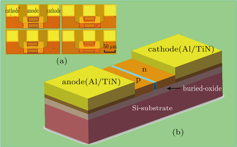 | Fig. 1. (color online) (a) Optical micrograph of the samples with different i-widths, and (b) geometric construction schematic diagram of p–i–n diode. |
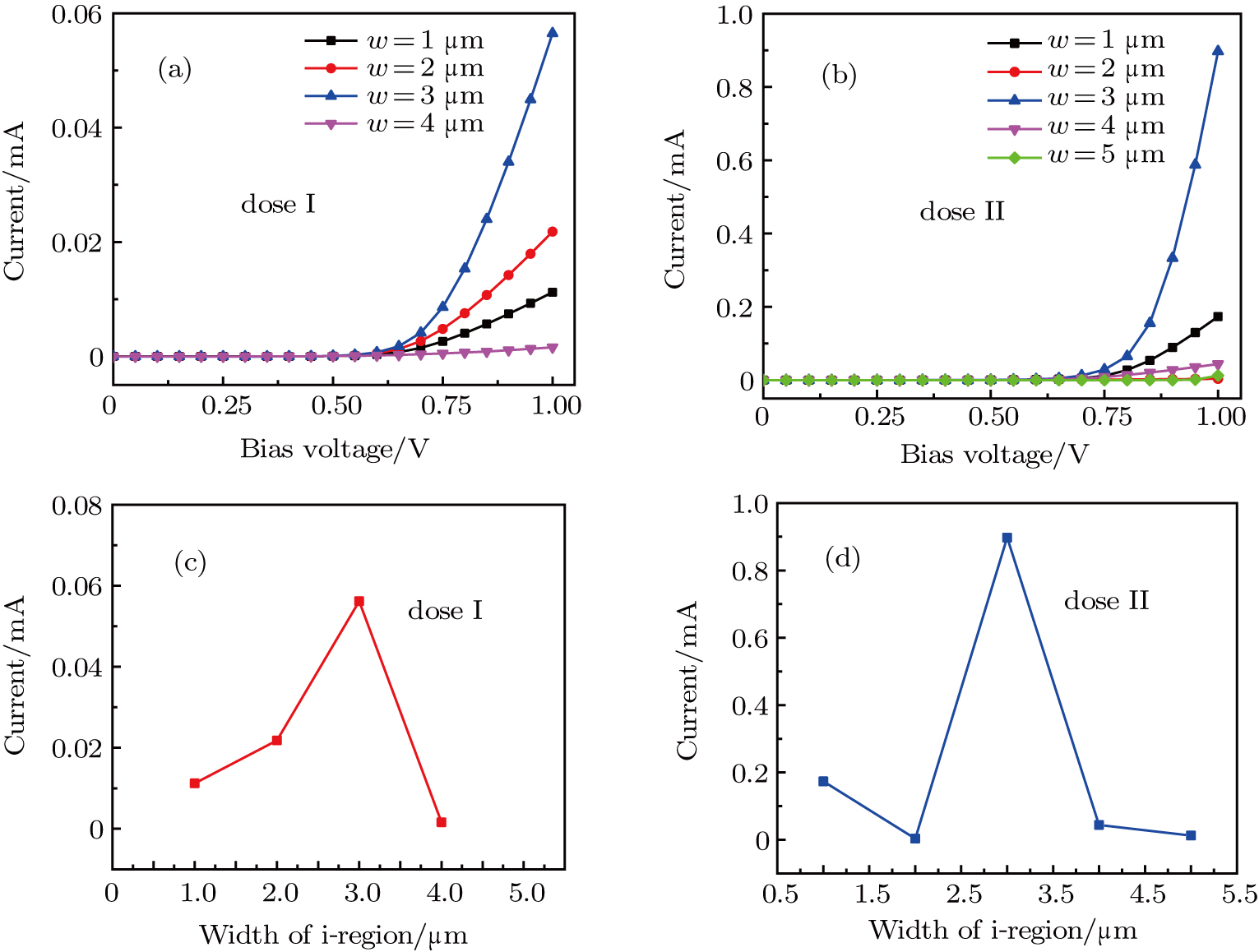
The I–V characteristics of the prepared samples are measured by a Keithley 4200. Figures
For the abnormal phenomenon, an analytical model of the current transport is set up to analyze the experimental results. In order to simplify our analysis, we make two appropriate assumptions. Firstly, assuming that neither traps nor impurities were introduced in the production process, so there is no trap-charge that participates in the carrier transportation. Secondly, both p-region and n-region are heavily doped and the i-region is intrinsic, therefore the widths of the space charge region in the p-region and n-region are too narrow to be neglected. Approximately, we assume that the i-region is depleting and the voltage mainly drops in the i-region: there is no voltage drop in the neutral zones in the p-region and n-region.
Figure
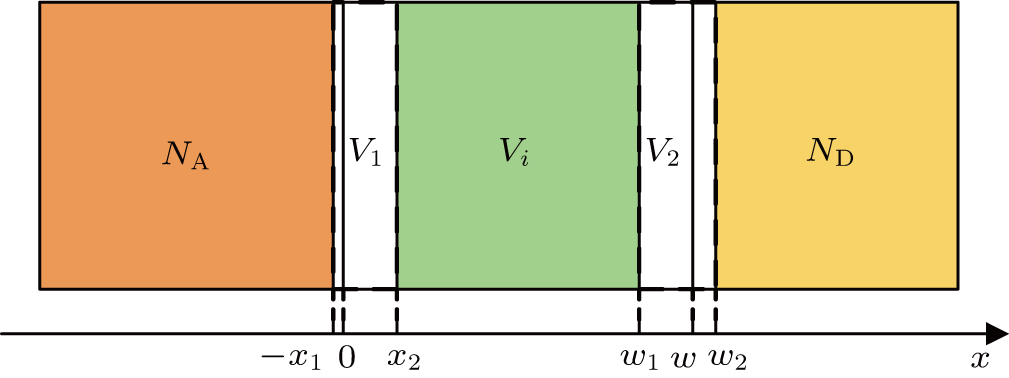 | Fig. 3. (color online) Pattern diagram of p–i–n diode. The doping concentrations of p- and n-layers are NA and ND, respectively. x = 0 and x = w are the doping boundaries. |
Our interest lies in the injected carrier distribution in the i-region. It should be noted that the two-type carriers share the same distribution profile in the i-region to keep the quasi-neutrality of this region p(x) = n(x).[9–11] With the aid of the coordinate system in Fig.

According to the Shockley diode model,[15] we think that hole injection current, electron injection current, and recombination current compose the total current. The hole injection current is the diffusion current at the n/i interface, and the electron injection current is the diffusion current at the p/i interface. By calculation, the three current components are obtained as follows:[10,13]
The inhomogeneous distribution of injected non-equilibrium carriers forms an electric field in the i-region. Therefore, the voltage Vi can be obtained from the integration of electric field E(x) over the i-region as follows:
With these equations, the total current density can be solved at any required applied voltage by a computer. The parameters used for the calculation are shown in Table
| Table 1.
Parameters used for calculation. . |
Figure
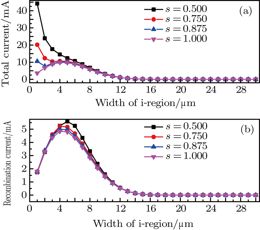 | Fig. 4. (color online) Plots of total (a) and recombination (b) currents versus i-layer thickness with different s values and ND = 8 × 1016 cm−3 at Vbias = 0.8 V. |
In addition, we calculate the recombination current (Fig.
The hole concentration distribution p(x) is shown in Fig.
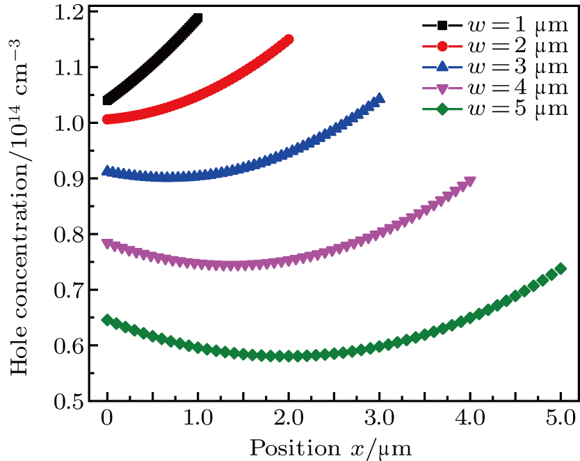 | Fig. 5. (color online) Plots of concentration distribution p(x) versus position in the intrinsic region of p–i–n junction with τ = 1 × 10⁻⁸ s and s = 0.875. |
As discussed before, the injected carriers present recombination in the i-region, and the recombination current plays a crucial role in abnormal phenomenon. Thus, we study the relationship between the current and the carrier lifetime. As shown in Fig.
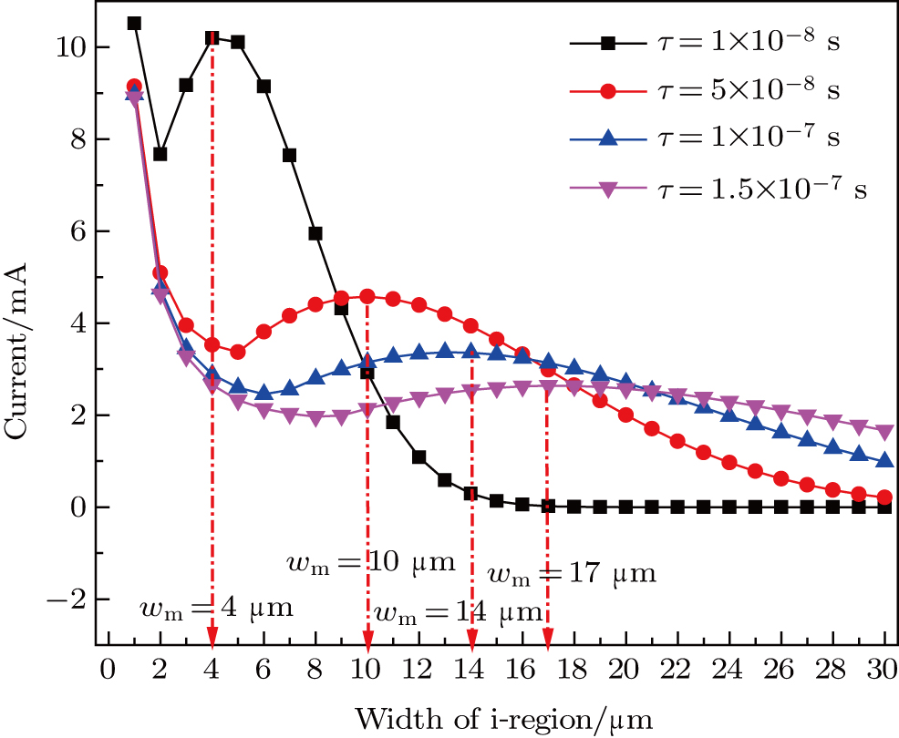 | Fig. 6. (color online) Plots of current versus i-region width for different carrier lifetimes (s = 0.875). |
When the carrier lifetime increases, less carriers present recombination and most carriers are injected into the boundary of the i-region. As a result, the injection current dominates the total current. With the increase of the width, it is difficult to inject the carriers into the boundary, so the recombination current regains its dominant function. Consequently, the critical width becomes bigger when the lifetime increases.
In the present work, the I–V characteristics of the p–i–n devices with different i-region widths have been investigated experimentally and theoretically. It is found that the current shows the non-monotonic behavior as a function of i-region width at a fixed voltage, which is a meaningful finding. In theoretical analysis, both the diffusion current and the recombination current are taken into account to refine the I–V characteristic of the p–i–n junction. For the non-monotonic behavior, the injection current plays an important role in the tiny i-region width, while the recombination current is dominated for the case of the large i-region width. On the other hand, the concentration ratio between p-region and n-region and carrier lifetime prove to be related to the experimental abnormal phenomenon. The concentration ratio has an influence on the variation trend of the curves, and the lifetime determines the critical width.
| [1] | |
| [2] | |
| [3] | |
| [4] | |
| [5] | |
| [6] | |
| [7] | |
| [8] | |
| [9] | |
| [10] | |
| [11] | |
| [12] | |
| [13] | |
| [14] | |
| [15] |


