


Influence of fin architectures on linearity characteristics of AlGaN/GaNFinFETs
Cite this Article
Liu Ting-Ting, Zhang Kai, Zhu Guang-Run, Zhou Jian-Jun, Kong Yue-Chan, Yu Xin-Xin, Chen Tang-Sheng. Influence of fin architectures on linearity characteristics of AlGaN/GaNFinFETs. Chinese Physics B, 2018, 27(4): 047307 
Permissions
Influence of fin architectures on linearity characteristics of AlGaN/GaNFinFETs
† Corresponding author. E-mail:
Abstract
We investigate the influence of fin architecture on linearity characteristics of AlGaN/GaNFinFET. It is found that the FinFET with scaled fin dimensions exhibits much flatter Gm characteristics than the one with long fins as well as planar HEMT. According to the comparative study, we provide direct proof that source resistance rather than tri-gate structure itself dominates the Gm behavior. Furthermore, power measurements show that the optimized FinFET is capable of delivering a much higher output power density along with significant improvement in linearity characteristics than conventional planar HEMT. This study also highlights the importance of fin design in GaN-based FinFET for microwave power application, especially high-linearity applications.
1. Introduction
Recently, GaNFinFETs or tri-gate HEMTs have drawn considerable attention because of their potential advantages over conventional planar HEMTs. Better suppression of short channel effects (SCEs) from enhanced gate control of additional sidewall gates,[1,2] and possible higher electron velocity[3] would enable further scaling of the gate length for high-speed device application. Besides, positive threshold voltage (VTH) shift and better electrostatics also make them a very promising candidate for the power electronics applications.[4,5] To date, there have been multiple demonstrations of GaNFinFETs with varied structures.[1–9] One of the key differences between them lies in the relative position between fins and gate electrode. As suggested by previous work, these fin variants are likely to bring a difference to Gm behavior and thus the linearity characteristics of devices. Azize et al. reported a broader Gm curve in a FinFET featuring nano-fins along the entire area between source and drain than in planar HEMTs.[7] Similarly, improvement in Gm flatness for Al(In)N/GaN fin-type HEMTs was also observed in Ref. [8] where the formed fins still extended beyond the gate region. On the other hand, extremely high linearity characteristics of Gm and fT were achieved by forming InAlN/GaN fins only under the gate electrode in a self-aligned way.[9] Recently, our group demonstrated a high-linearity AlGaN/GaNFinFET by developing new fin formation sequences.[10] With regard to microwave applications, a direct comparison between these FinFETs is imperative in order not only to get more insight into various properties of GaNFinFETs but also to determine the optimal fin configuration with the best linearity behavior. However, these efforts are not available at the moment.
In this work, we investigate comparatively two varied AlGaN/GaN fin architectures fabricated in different processes. One FinFET features long fins extending beyond the gate footprint, whereas the other one has fins fully covered by the gate electrode. The latter FinFET is found to exhibit an enhanced direct current (DC), power and linearity performance. The possible origin of Gm nonlinearity behavior is also analyzed.
2. Experimental details
The epitaxial structure consists of an Al0.3Ga0.7N (11 nm)/AlN (1 nm) barrier layer, a 20-nm GaN channel, and a 1.0-
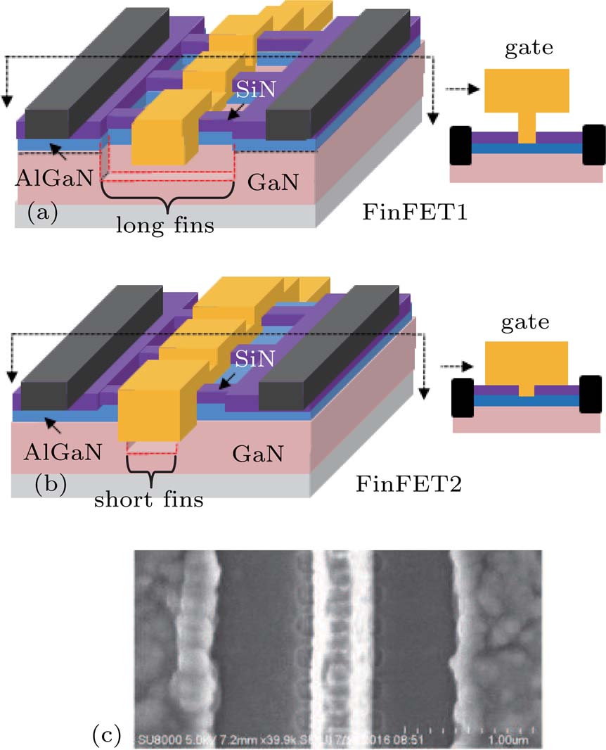
For the first structure, denoted as FinFET1, a low-damage BCl3/Cl2 plasma dry etching was subsequently performed, resulting in a 600-nm-long Si3N4/AlGaN/GaN fin. The AlGaN/GaN heterostructure was etched to a targeted 30-nm depth. Then, a T-type gate was determined by EBL using a bilayer resist. Finally, after removing Si3N4 dielectric under the gate footprint by SF6-based plasma etching, an Ni/Au gate metal was evaporated and lifted off.
On the other hand, for FinFET2, after the above-mentioned Si3N4 mask transfer, the gate footprint was first determined by a second EBL. Then, the etching of AlGaN/GaN was carried out with the same depth as that for the FinFET1. Finally, following SiN mask removal from the top of the fin by SF6-based plasma, a 450-nm-long gate electrode fully covering the fin region was determined by a third EBL. It is noteworthy that this implementation of gate footprint definition prior to AlGaN/GaN etching allows FinFET2 to have scaled nano-fins as long as the gate length. In contrast, the fabricated fins in FinFET1 extended to the source/drain access region for a total of ∼500 nm, which leads to a relatively large parasitic source resistance.
The structures are schematically shown in Fig. 


 | Fig. 1. (color online) Schematics of (a) FinFET1 and (b) FinFET2, (c) SEM image of FinFET2 after gate formation. The difference in gate geometry is also indicated. |
3. Results and discussion
The direct current (DC) output characteristics of planar HEMT and FinFETs are plotted in Fig. 


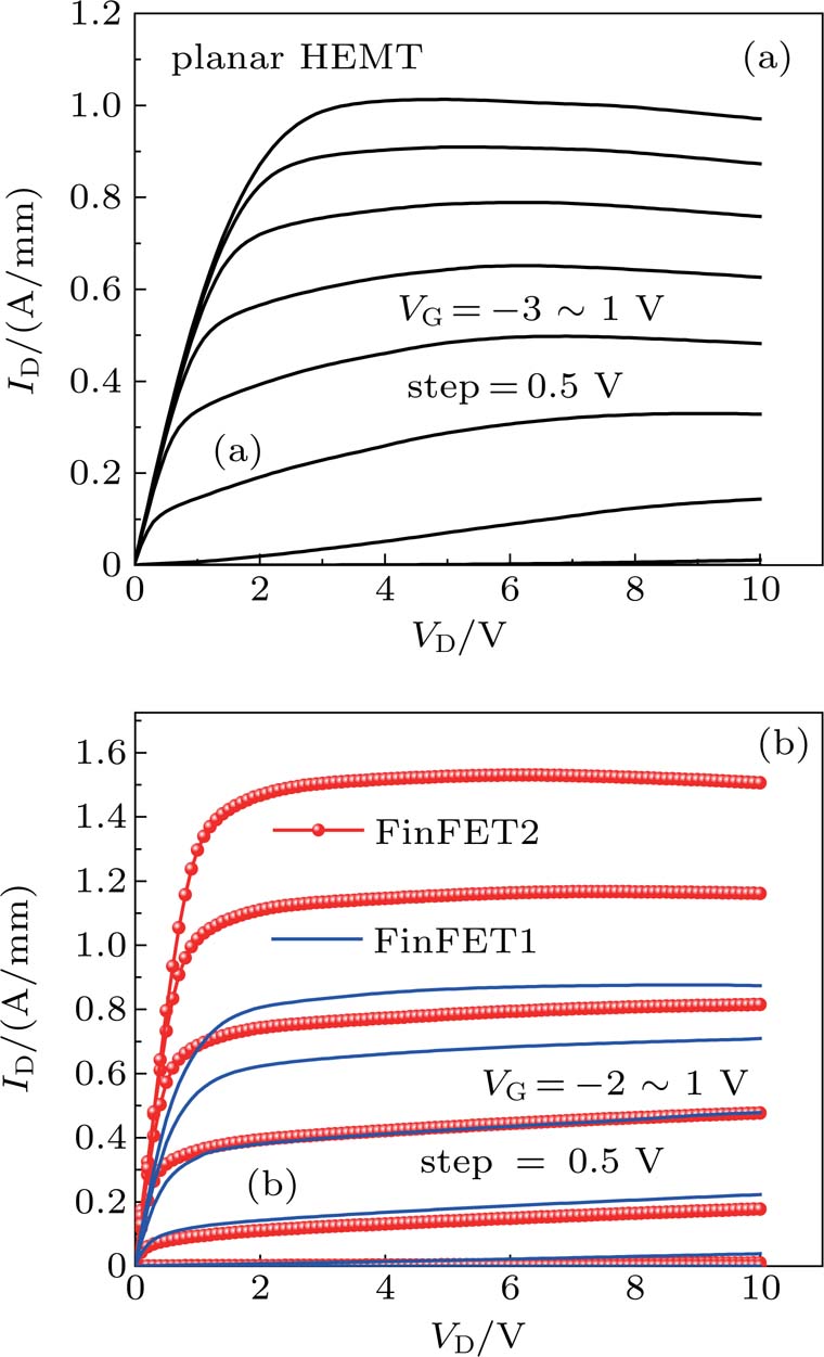 | Fig. 2. (color online) Typical normalized ID–VD curves of (a) planar HEMT and (b) FinFETs each with a gate length of 100 nm. |
Figure 

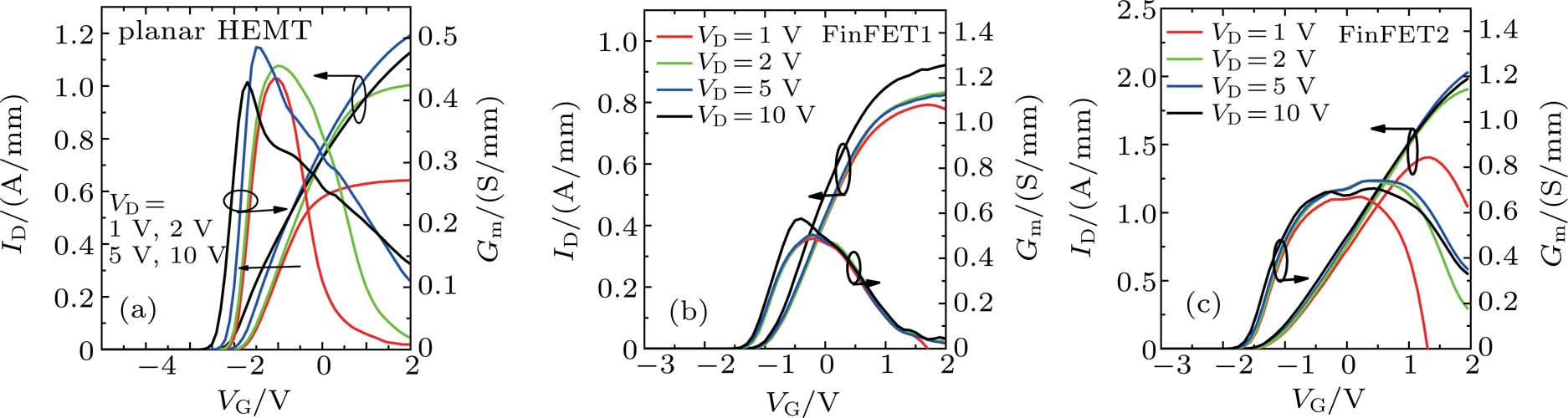 | Fig. 3. (color online) Transfer characteristics of (a) planar HEMT, (b) FinFET1, and (c) FinFET2 as a function of drain voltage at 
|
The values of differential source resistance (RS) of these devices as a function of drain current are measured to investigate the possible origin of this difference. The gate contact is forward biased with respect to the channel by introducing a 5-mA/mm current through the gate of the transistor into the channel as shown in the inset of Fig.
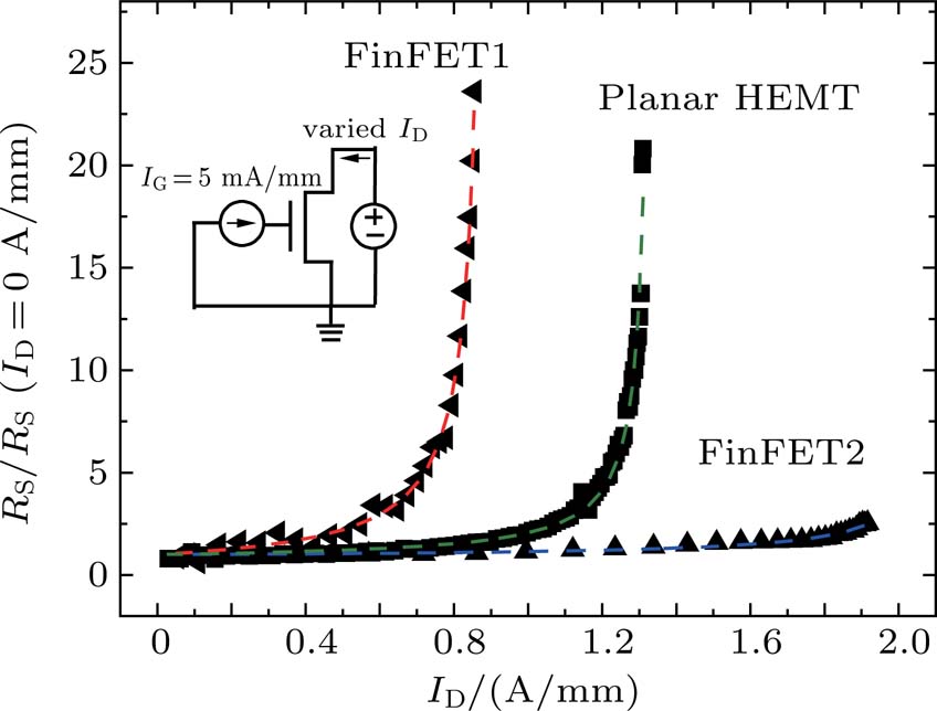 | Fig. 4. (color online) Comparison among normalized source resistances as a function of drain current density for all investigated devices. |
Sub-threshold characteristics as a function of drain voltage are displayed in Fig.
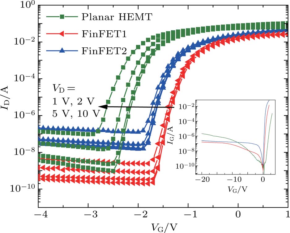 | Fig. 5. (color online) Sub-threshold characteristics of three types of devices investigated. Raw current values are given for clear comparison. Inset: gate diode leakage characteristics. |
The S parameters are measured on-wafer from 10 MHz to 40 GHz, and the resulting fT values are shown in Fig.
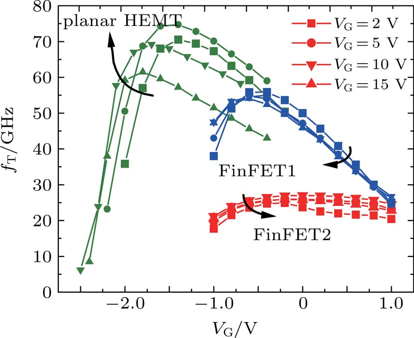 | Fig. 6. (color online) Changes of fT with gate and drain voltage. |
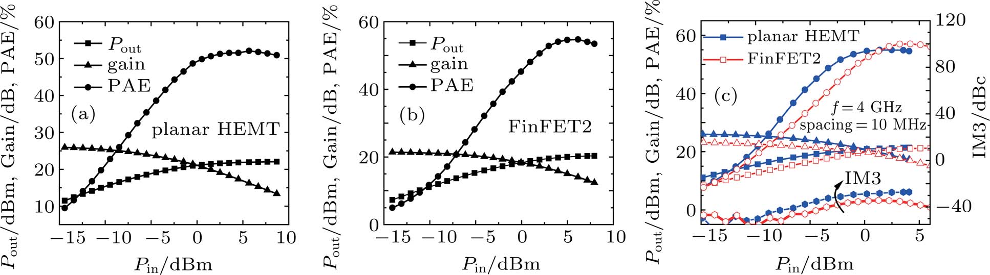
Since FinFET1 exhibits a similar Gm behavior but inferior DC performance in comparison with planar HEMTs, we conduct a comparison of the power performance between planar and FinFET2. Both single and two-tone RF power measurements are performed by a Maury Load–Pull system at 4 GHz. Both devices are biased at a drain voltage of 15 V in class AB using a quiescent drain current of 10% 

 | Fig. 7. (color online) (a) Large-signal output power characteristics of (a) planar HEMT, (b) FinFET2, and (c) two-tone linearity measurements conducted at 4 GHz with 10-MHz tone spacing. |
4. Conclusions and perspectives
A comparison of two types of fin architectures has been performed in this work. The SCEs and gate leakage properties are improved for both FinFETs in comparison with planar HEMT. However, the FinFET featuring nano-fins fully covered by a T-gate electrode allows higher values of Gm and 
Reference
| [1] | |
| [2] | |
| [3] | |
| [4] | |
| [5] | |
| [6] | |
| [7] | |
| [8] | |
| [9] | |
| [10] | |
| [11] | |
| [12] | |
| [13] | |
| [14] |