Effects of rapid thermal annealing on crystallinity and Sn surface segregation of Ge 1 x Sn x films on Si (100) and Si (111)
Miao Yuan-Hao†, , Hu Hui-Yong‡, , Song Jian-Jun, Xuan Rong-Xi, Zhang He-Ming
Key Laboratory of Wide Band-Gap Semiconductor Materials and Devices, East Main Building, School of Microelectronics, Xidian University, Xi’an 710071, China


† Corresponding author. E-mail: 15336118340@163.com huhy@xidian.edu.cn

Abstract

Germanium-tin films with rather high Sn content (28.04% and 29.61%) are deposited directly on Si (100) and Si (111) substrates by magnetron sputtering. The mechanism of the effect of rapid thermal annealing on the Sn surface segregation of Ge1 −xSnx films is investigated by x-ray photoelectron spectroscopy (XPS) and atomic force microscopy (AFM). The x-ray diffraction (XRD) is also performed to determine the crystallinities of the Ge1−xSnx films. The experimental results indicate that root mean square (RMS) values of the annealed samples are comparatively small and have no noticeable changes for the as-grown sample when annealing temperature is below 400 °C. The diameter of the Sn three-dimensional (3D) island becomes larger than that of an as-grown sample when the annealing temperature is 700 °C. In addition, the Sn surface composition decreases when annealing temperature ranges from 400 °C to 700 °C. However, Sn bulk compositions in samples A and B are kept almost unchanged when the annealing temperature is below 600 °C. The present investigation demonstrates that the crystallinity of Ge1−xSnx/Si (111) has no obvious advantage over that of Ge1−xSnx/Si (100) and the selection of Si (111) substrate is an effective method to improve the surface morphologies of Ge1−xSnx films. We also find that more severe Sn surface segregation occurs in the Ge1−xSnx/Si (111) sample during annealing than in the Ge1−xSnx/Si (100) sample.

PACS: 73.61.At
1. Introduction

Germanium-tin (Ge1−xSnx) alloys are of great research interest due to the fact that their bandgap structures can be tuned by varying the Sn content, which are essential for Si-based monolithic optoelectronic.[15] Both the theoretical and experimental studies have shown that Ge, an indirect-gap semiconductor, can be transferred into a direct-gap semiconductor with Sn content up to 6% or 10%. Such alloys have higher carrier mobility than Ge, which makes it suitable to serve as channel material for metal oxide semiconductor (MOS) devices[611] and tunnel field-effect transistors (TEFT).[12,13] Besides, Ge1−xSnx-based optoelectronic devices are compatible with the traditional Si CMOS process. Numerous growth methods, such as chemical vapor deposition (CVD),[1416] molecular beam epitaxy (MBE),[1719] solid phase epitaxy (SPE),[20] and pulsed laser deposition (PLD)[21] have been employed to grow Ge1−xSnx films. Compared with other growth methods, magnetron sputtering is one of the low-cost methods to deposit thin-film material. The greatest advantage of the magnetron sputtering is that the deposition rate and growth temperature can be regulated separately, which leads to the depositions of Ge1−xSnx films at a reasonable growth rate at a growth temperature as low as 150 °C. In addition, Ge target and Sn target are much safer than poisonous gas precursors, such as GeH4, Ge2H6, SnD4 or SnCl4.

Several groups have grown Ge1−xSnx alloys by magnetron sputtering. Tsukamoto et al. have presented crystalline Ge1−xSnx films on Si (100) substrates by magnetron sputtering at high growth temperature and high deposition rate.[22] Zheng et al. have reported Ge1−xSnx p-i-n photodetectors with Ge1−xSnx film deposited by magnetron sputtering.[23]

Meanwhile, there are several challenges in fabricating Ge1−xSnx films mainly due to the very low solid solubility (less than 1% of Sn in Ge) and the large lattice mismatch between Sn and Ge (approximately 15%), which makes it hard to grow Ge1−xSnx films with low defect density. What is more, Sn has a low surface energy compared with Si and Ge, which leads to Sn segregating from the surface of Ge1−xSnx alloy during epitaxial growth and thermal annealing. At a high Sn composition, the Sn surface composition of the film becomes heterogeneous due to the fact that Sn tends to segregate from the surface of the film, which is harmful for the performance of the device. Good knowledge of the mechanism of the effects of post-annealing on the crystallinity and Sn surface segregation of Ge1−xSnx films is essential for fabricating the high-crystallinity Ge1−xSnx films. Therefore, it is urgently needed to fabricate Ge1−xSnx films with high Sn content and no Sn segregation.Tsukamoto et al. have investigated the Sn surface segregation with low Sn content during MBE epitaxial growth.[24] Sn migration control at high temperature due to high deposition speed was discussed.[25] The thermal stability of Ge1−xSnx films during annealing has also been reported.[2629] Among these researches, Sn surface segregations of high-Sn- content Ge1−xSnx films on Si (100) and Si (111) have not been extensively investigated in detail.

In this study, we prepare Ge1−xSnx films on Si (100) and Si (111) substrates with Sn content up to 28.04% and 29.61%, followed by post-annealing at the temperature ranging from 300 °C to 700 °C. The effects of thermal rapid annealing on the Sn surface segregation of Ge1−xSnx films on Si (100) and Si (111) are investigated in detail. Several characterization methods are employed to discuss the crystallinities and Sn surface segregations of Ge1−xSnx films, including x-ray diffraction (XRD), atomic force microscopy (AFM), and x-ray photoelectron spectroscopy (XPS).

2. Experiment

The Ge1−xSnx thin films were deposited directly on 4-inch n-type Si substrates by magnetron sputtering with using high-purity Ge target (99.999% purity, 50.8 mm diameter) and Sn target (99.999% purity, 50.8 mm diameter). The distance between the targets and substrates was about 150 mm. Prior to depositing the thin films, Si (100) and Si (111) substrates were cleaned sequentially by acetone, ethanol and immersed in a 1:10 = HF:H2O for 1 min to remove the native oxides from the Si substrate. Finally, the substrates were rinsed in deionized water and dried by pure N2. After loading them into the growth chamber, the chamber was pumped down to (1 Torr = 1.33322×10² Pa) as the base pressure. The substrates were heated to 150 °C before depositing the crystalline Ge1−xSnx films. During the deposition, the sputtering pressure was kept at 7 mTorr by utilizing argon. The compositions of Ge and Sn in the films were controlled by maintaining a DC power of 100 W for the Ge target and varying the power of the Sn target.

To improve the crystallinities of the films, the 4-inch (1 inch = 2.54 cm) Si substrates along with the Ge1−xSnx films were cut into pieces for different thermal annealing temperatures ranging from 300 °C to 700 °C for 30 s in the RTP150. Pure N2 was chosen as the annealing atmosphere to avoid any effect originating from O2. The as-grown Sn mole fractions of samples were approximately 28.04% and 29.61%, respectively, as determined by XPS. In order to verify the effects of post-annealing on the crystallinity and Sn surface segregation of Ge1−xSnx films grown on Si substrates, AFM images and XRD scans were conducted.

3. Results and discussion

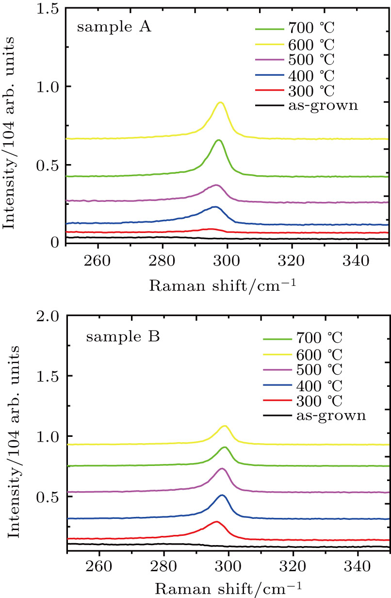
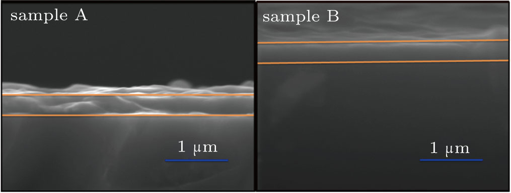
Information about crystal orientation, Ge1−xSnx layer thickness, annealing temperature, FWHM (°), Raman peak shift (cm−1), and strain degree ε (%) of each sample are presented in Table 1. The thickness values of the Ge1−xSnx films are determined by SEM to be 300 nm and 300 nm for samples A and B, respectively (Fig. 1). For high-Sn-composition Ge1−xSnx alloys, a detailed comparison study of the Poisson rate is lacking, the strain degree ε (%) of each example is determined by Raman spectra that are shown in Fig. 4.

Fig. 1. (color online) Cross-sectional SEM image of samples A and B.
Table 1.

Crystal orientations, values of Ge1−xSnx layer thickness (nm), annealing temperature, FWHM (°), Raman peak shift (cm−1), and ε (%) for each sample.

.

The XRD measurements of the Ge1−xSnx thin films with high Sn compositions are performed to investigate the effects of the post-annealing on the crystallinity of the Ge1−xSnx films. The XRD curves of sample A annealed at various temperatures are shown in Fig. 2. The diffraction peaks of Ge1−xSnx/Si (100) and Sn(420) could be observed for all of the samples annealed at the temperatures ranging from 300 °C to 700 °C. The Sn (420) peak almost satisfies the standard angle of 72.424 °C, and peaks from the Ge1−xSnx films are diffracted at 64 °C. A comparison between the as-grown sample and the sample annealed at 300 °C shows that the XRD peak positions due to the Ge1−xSnx/Si (100) films remain almost the same, indicating there is little change in the bulk composition. In addition, a notable right shift of the Ge1−xSnx/Si (100) diffraction peak is observed for the sample annealed at 700 °C.
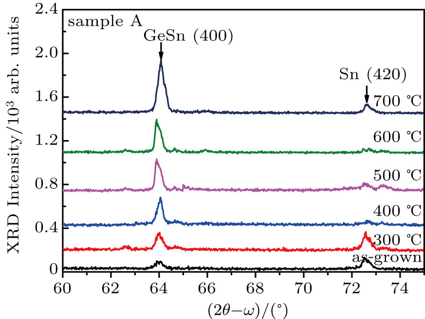
Fig. 2. (color online) XRD patterns of the crystalline Ge1−xSnx/Si (111) film after RTA at 300 °C, 400 °C, 500 °C, 600 °C, and 700 °C for 30 s.

The XRD curves of the sample B annealed at various temperatures are shown in Fig. 3. The diffraction peaks of Ge1−xSnx/Si (111), Sn (200) and Sn (100) can be seen for all of the samples. The Sn (200), and Sn (101) peaks almost satisfy the standard angles of 30.639 °C and 32.019 °C. Contrary to what we expected, XRD peaks of Ge1−xSnx/Si (111) shift toward the right at the annealing temperature as low as 400 °C and bulk Sn compositions in Ge1−xSnx/Si (111) films decrease dramatically. Combining Fig. 2 with Fig. 3, XRD peak intensities and FWHMs of samples A and B are found to be almost the same, indicating that the crystallinity of Ge1−xSnx/Si (111) has no obvious advantages over that of Ge1−xSnx/Si (100). The right shifts of the Ge1−xSnx/Si (111) diffraction peak are observed for the sample annealed at 500 °C, 600 °C, and 700 °C, respectively. We assume that the right shift of the Ge1−xSnx peak may be due to the combined action of Sn surface segregation and the strain relaxation in Ge1−xSnx. Hence, we measure the Raman spectra of samples A and B to determine the strain relaxation in the films, which are presented in Fig. 4.
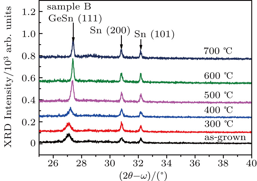
Fig. 3. (color online) XRD patterns of the crystalline Ge1−xSnx/Si (111) film after RTA at 300 °C, 400 °C, 500 °C, 600 °C, and 700 °C for 30 s.
Fig. 4. (color online) Raman spectra of sample A and B annealed at the temperatures ranging from 300 °C–700 °C.

The peak shift compared with Ge–Ge Raman peak (300 cm−1) from bulk Ge can be calculated from the following equation[3032] where a = −82 cm−1 and b = −563 cm−1. The Sn composition of the Ge1−xSnx film is measured by XPS, and the strain in the film is determined by Eq. (1). We find that the strain relaxation does not vary obviously with annealing temperature in the Ge1−xSnx film, which indicates that the right shift of the Ge1−xSnx peak is mainly due to the Sn surface segregation.

As the thickness of GeSn layer is far beyond the critical thickness,[32] the Sn composition can be calculated from Eqs. (2)–(5) by simply assuming that the GeSn film is fully relaxed. Sn bulk composition in Ge1−xSnx film can be determined by the following relationship: where is the lattice parameter of the Ge1−xSnx alloy, is the lattice parameter of the Sn ( ), is the lattice parameter of the Ge ( ), b is the bowing parameter, and x is the Sn bulk composition of the Ge1−xSnx film. Bragg’s law is used to extract the out-of-plane lattice parameter of the Ge1−xSnx film. We can now calculate the out-of-plane lattice parameters of the Ge1−xSnx/Si (100) and Ge1−xSnx/Si (111) Eqs. (2) and (3). where λ = 0.15406 nm and θ hkl is the Bragg angle of the Ge1−xSnx layer peak.

Thus, Sn bulk composition of the Ge1−xSnx film can be obtained from

The effects of post-annealing on the surface morphology and Sn surface composition are identified by AFM and XPS, respectively.

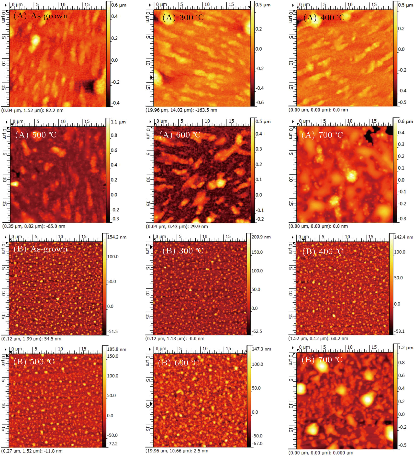
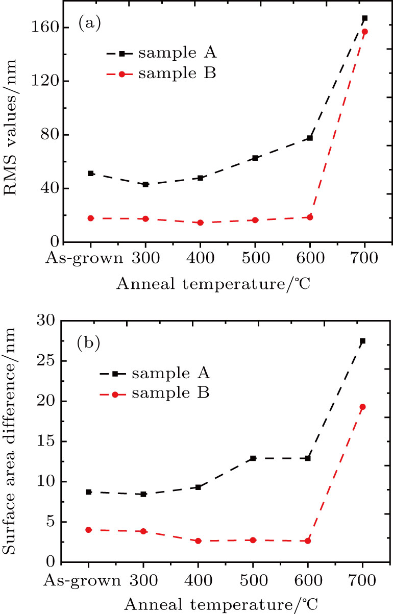
Typical AFM images of samples A and B annealed at temperatures ranging from 300 °C to 700 °C are shown in Fig. 4. The RMS values of all the samples are extracted from AFM surface scans. For sample A, the strain degree of the as-grown one is −0.053% and the diameter of the largest Sn 3D island is . When the annealing temperature is below 400 °C, the surface roughness of the annealed sample has no noticeable change compared with that of the as-grown sample and the strain in the films remains almost unchanged. When the annealing temperature is 700 °C, the diameter of the Sn-rich island (700 °C, ) becomes larger than that of the as-grown one. What is more, the strain degree of the film is −0.038%. For sample B, the strain degree of the as-grown one is −0.052% and the diameter of the largest Sn 3D island is . When the annealing temperature is below 600 °C, the surface roughness values of the annealed samples have no noticeable changes compared with that of the as-grown sample. When there is an increase in annealing temperature, the diameter of Sn-rich island(700 °C, ) becomes larger than that of the as-grown one. Figure 6(a) shows the variations of RMS value with anneal temperature. For sample A, there is a small decrease in RMS when the annealing temperature rises to 300 °C, which means that 300 °C may be responsible for the improvements of surface morphologies of the Ge1−xSnx/Si (100) layers. With the further increase of the annealing temperature, the RMS value rises almost linearly. Meanwhile, the RMS value of sample B remains almost unchanged at various annealing temperatures ranging from 300 °C to 600 °C but goes up rapidly as temperature increases from 600 °C to 700 °C, which coincides with the XRD results.

Fig. 5. (color online) AFM surface scans ( ) of the samples annealed at various temperatures for 30 s.
Fig. 6. (color online) Plots of (a) RMS and (b) SAD versus annealing temperature for samples A and B, respectively, which are extracted from AFM images. SAD is the surface area difference of Ge1−xSnx films.

Figure 6(b) demonstrates the surface area differences (SAD) of samples A and B annealed at various temperatures, which shows that the thermal stability of surface morphology of Ge1−xSnx/Si (111) is better than that of Ge1−xSnx/Si (100) from 300 °C to 600 °C. As is well known, discontinuity spacing of the Si (111) plane is larger than that of the Si (100) plane. Thus, the Ge1−xSnx alloy is more likely to be formed on Si (111) substrate, which indicates that the selection of Si (111) is an effective method to reduce the surface roughness values of Ge1−xSnx films.

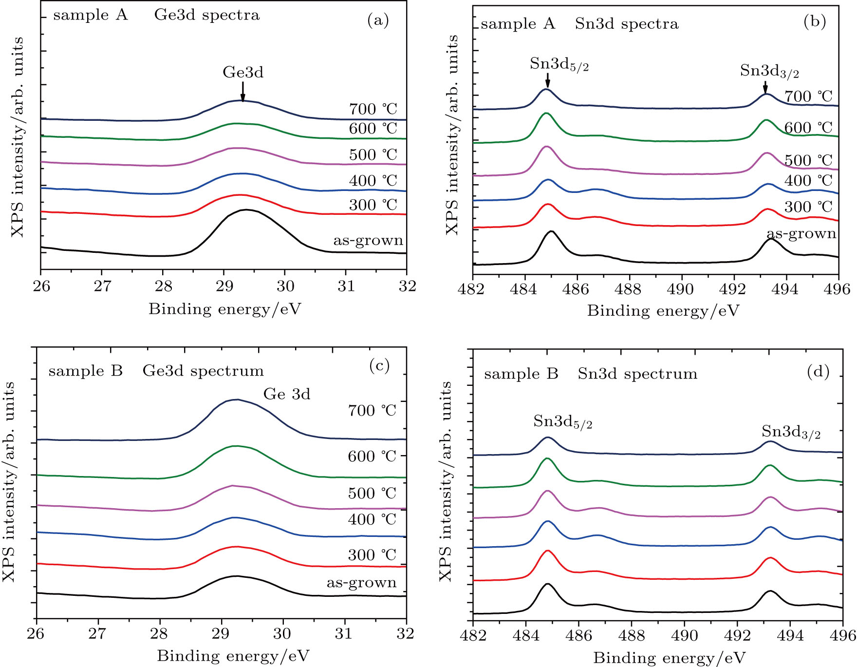
Therefore, it can be assumed that the Sn surface composition of the film will increase at a higher annealing temperature. In order to further verify this assumption, extensive XPS measurement is carried out and it is a more quantized method to determine the changes of near surface composition in the thin films. Monochromatic carbon (C) is used to calibrate the position of binding energy. In order to remove any contaminants from the surfaces of the Ge1−xSnx layers, all the samples are placed into a K-Alpha XPS system after being etched for 30 s. The XPS spectra of Ge3d and Sn3d before and after being annealed at different temperatures are plotted in Fig. 7, showing that the peak with a binding energy of 29.1 eV is corresponding to the Ge3d, while the peaks with binding energies of 484.9 eV and 493.3 eV are corresponding to Sn3d5/2 and Sn3d3/2.

Fig. 7. (color online) Ge3d and Sn3d XPS spectra of samples A and B alloys annealed at different temperatures for 30 s. Each curve is stacked for clarity. Ge3d and Sn3d peaks are marked by downward arrows.

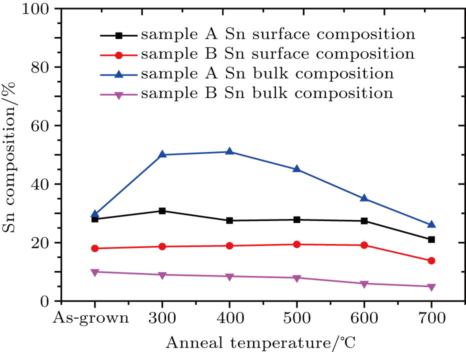
Contrary to what we assumed, the Sn surface compositions of the films decrease with annealing temperature increasing when the annealing temperature is above 300 °C. For sample A annealed at 400 °C, 500 °C, and 600 °C, Sn surface compositions are 27.5%, 27.8%, and 27.6% (Fig. 8) and RMS values of GeSn/Si (100) are increasing (Fig. 6). For sample B annealed at 400 °C, 500 °C and 600 °C, Sn surface compositions are 50%, 45%, and 30% (Fig. 7). However, the RMS values of GeSn/Si (111) remain almost unchanged with annealing temperature increasing up to 600 °C (Fig. 6). We believe that the Sn surface composition decreases with the annealing temperature increasing up to the melting points of Sn (232 °C), which may be due to the Sn desorption from the surface. A higher annealing temperature may increase the desorption rate of Sn, which is also found in[26]. The Sn surface composition decreases when the annealing temperature is 400 °C, which can be attributed to the formation of Sn desorption. When the annealing temperature is 500 °C, Sn surface compositions decrease to 27.8% and 45% for Ge1−xSnx/Si (111) and Ge1−xSnx/Si (100), respectively. RMS values of GeSn/Si (100) increase with annealing temperature increasing up to 600 °C. However, the RMS values of GeSn/Si (111) remain almost unchanged for the as-grown sample when the annealing temperature goes up to 600 °C (Fig. 6). Comparing Sn surface compositions with Sn bulk compositions, Sn bulk compositions in samples A and B are kept almost unchanged when the annealing temperature is below 600 °C. When the annealing temperature is 700 °C, Sn bulk composition decreases slightly and the diameter of Sn 3D island becomes larger than that of the as-grown sample. We also find that the variation of Sn surface composition in sample B is much larger than in sample A, which suggests that more severe Sn surface segregation occurs in the Ge1−xSnx/Si (111) sample during annealing compared with in the Ge1−xSnx/Si (100) sample. That the areal density of Si (111) is larger than the areal density of Si (100) leads to the identity distance of GeSn/Si (111) being larger than that of GeSn/Si (100). In addition, a larger identity distance contributes to the smaller interfacial gravity, which may make more severe Sn surface segregation occur in the GeSn/Si (111) sample.

Fig. 8. (color online) Sn surface compositions and Sn bulk compositions measured by XPS and XRD as a function of annealing temperature for samples A and B.
4. Conclusions

In this work, crystalline Ge1−xSnx films are grown on Si (100) and Si (111) substrate under 150 °C by magnetron sputtering. The XRD scans are performed to determine the crystallinities of Ge1−xSnx/Si (111) and Ge1−xSnx/Si (100). It is concluded that the crystallinity of Ge1−xSnx/Si (111) has no obvious advantage over that of Ge1−xSnx/Si (100). The thermal stability of the surface morphology of Ge1−xSnx/Si (111) is better than that of Ge1−xSnx/Si (100) and Sn surface composition decreases when annealing temperatures range from 400 °C to 700 °C. A higher annealing temperature may contribute to the formation of Sn desorption. However, Sn bulk compositions in samples A and B are kept almost unchanged when the annealing temperature is below 600 °C. Furthermore, more severe Sn surface segregation occurs in the Ge1−xSnx/Si (111) sample during annealing than in the Ge1−xSnx/Si (100) sample. These results reveal that an increasing annealing temperature causes Sn to form clusters and contributes to the Sn atoms moving to the surface of Ge1−xSnx thin film. Restricting the Sn atoms moving to the surface can restrain the Sn surface segregation.

Reference
[1] Wirths S Geiger R 2015 Nat. Photon. 9 88
[2] Dutt B Lin H 2013 IEEE J. Sel. Topi. Quantum Electron. 19 1502706
[3] Homewood K P Lourenço M A 2015 Nat. Photon. 9 78
[4] Ghetmiri S A Du W 2014 Appl. Phys. Lett. 105 151109
[5] Du W Ghetmiri S A 2014 Appl. Phys. Lett. 105 051104
[6] Gong X Han G 2013 IEEE Electron. Dev. Lett. 34 339
[7] Liu Y Yan J 2014 IEEE Trans. Electron. Dev. 61 3639
[8] Schulte-Braucks C Von d D N 2016 ACS Appl. Mater. Interfaces 8 13133
[9] Hart J Adam T 2016 J. Appl. Phys. 119 093105
[10] Liu M S 2014 IEEE Symposium on VLSI Technology 100
[11] Han G Q 2011 Technical Digest- International Electron Devices Meeting, IEDM 16.7.1
[12] Wang H 2016 IEEE Trans. Electron Dev. 63 303
[13] Liu M 2015 IEEE Trans. Electron Dev. 62 1262
[14] Senaratne C L Gallagher J D 2014 J. Appl. Phys. 116 133509
[15] Zelazna K Polak M P 2015 Appl. Phys. Lett. 106 142102
[16] Wang W Vajandar S 2016 J. Appl. Phys. 119 155704
[17] MeeYi Ryu Harris T R 2013 Appl. Phys. Lett. 102 171908
[18] Zhang D Jin L 2016 J. Alloys. Compd. 665 131
[19] Sadoh Taizoh Ooato Akira Park Jong Hyeok 2015 Thin Solid Films 602 20
[20] Tran T T Pastor D Gandhi H H 2016 J. Appl. Phys. 119 78
[21] Huang Z M Huang W Q Liu S R 2016 Sci. Rep. 6 24802
[22] Tsukamoto T Hirose N Kasamatsu A 2015 J. Mater. Sci. 50 4366
[23] Zheng J Wang S Liu Z 2016 Appl. Phys. Lett. 108 4532
[24] Tsukamoto T Hirose N Kasamatsu A 2015 Appl. Phys. Lett. 106 133506
[25] Taoka N Capellini G Nils V D D 2016 Appl. Phys. Express 9 0312
[26] Wang W 2014 Appl. Surf. Sci. 321 240
[27] Wang W 2016 J. Phys. D: Appl. Phys. 49 225102
[28] Li H 2014 Appl. Phys. Lett. 105 151906
[29] Lin H Chen R 2011 Appl. Phys. Lett. 98 261917
[30] Zhang L 2016 J. Non-Cryst. Solids 448 74
[31] Lin J Q 2013 ECS J. Solid State Sci. Tech. 2 P138
[32] Wang W 2015 Appl. Phys. Lett. 106 232106