Angle-resolved x-ray photoelectron spectroscopy study of GeOx growth by plasma post-oxidation
Zhao Zhiqian1, Zhang Jing1, †, Wang Xiaolei2, 3, ‡, Wei Shuhua1, Zhao Chao2, 3, Wang Wenwu2, 3
Microelectronics Department, North China University of Technology, Beijing 100041, China
Key Laboratory of Microelectronics Devices & Integrated Technology, Institute of Microelectronics, Chinese Academy of Sciences, Beijing 100029, China
School of Microelectronics, University of Chinese Academy of Sciences, Beijing 100049, China


† Corresponding author. E-mail: zhangj@ncut.edu.cn wangxiaolei@ime.ac.cn

Abstract

The growth process of GeOx films formed by plasma post-oxidation (PPO) at room temperature (RT) is investigated using angle-resolved x-ray photoelectron spectroscopy (AR-XPS). The experimental results show that the distributions of the Ge4+ states, a mixture of the Ge2+ and Ge3+ states, and the Ge+1 states are localized from the GeOx surface to the GeOx/Ge interface. Moreover, the Ge+1 states are predominant when the two outermost layers of Ge atoms are oxidized. These findings are helpful for establishing in-depth knowledge of the growth mechanism of the GeOx layer and valuable for the optimization of Ge-based gate stacks for future complementary metal–oxide–semiconductor (MOS) field-effect transistor (CMOSFET) devices.

1. Introduction

As Si transistor technology advances beyond the 10-nm node, it has been more difficult to further enhance the performance of MOSFETs on the Si platform owing to the inherent limitations of the Si material itself. The device research community is increasingly paying close attention to the replacement of Si in the transistor channel with novel and high-mobility materials.[1,2] Among several possible candidate materials, Ge is a promising material that can offer increases in the electron and hole mobilities by factors of approximately two and four, respectively, compared with those of Si and can provide compatibility with conventional Si integration technologies.[1,3,4] However, several issues still need to be resolved before Ge can be completely applied to field-effect transistors (FETs) as a proven technology to attain a high performance. One of the critical issues is to provide a high-quality interfacial layer, which can avoid causing a substantial degradation in the drive current in both the low equivalent oxide thickness (EOT) and short-channel regimes.[3]

Recently, wide ranges of materials and processes have been researched to achieve superior Ge surface passivation, including nitride,[511] Si,[1215] S,[1620] and Ge dioxide or suboxide (GeOx)[2038] passivation layers. High-quality GeO2 has recently been reconsidered as a promising passivation layer owing to its extremely low Dit (∼ 6 × 10¹⁰ eV−1·cm−2)[39] and its potential to enable high-performance Ge n-MOSFETs.[40] GeO2 or GeOx can be grown by thermal oxidation at atmospheric pressure[21,22] and high pressure (∼ 70 atm; 1 atm = 1.01325 × 10⁵ Pa),[23,24] respectively, as well as plasma post-oxidation (PPO)[3338,4146] or ozone oxidation.[2932] Lee et al.[24] proposed a two-step oxidation process with high-pressure (70 atm) oxidation and low-temperature oxygen annealing to form an ideal GeO2/Ge stack based on thermodynamic and kinetic control. A GeO2 thickness of about 20 nm and Dit < 1011 eV−1 · cm−2 near the midgap were obtained with a peak electron mobility of 1100 cm2 · V−1·s−1. Kuzum et al.[30] used ozone oxidation to grow GeOx and achieved a mobility that is ∼ 1.5 times higher than the universal Si mobility. Zhang et al.[37] demonstrated that by using the electron cyclotron resonance oxygen PPO method, the EOT of the HfO2/Al2O3/GeOx/Ge gate stack can be scaled down to 0.7 nm–0.8 nm while maintaining Dit at a level of 1011 eV−1·cm−2. Further, the peak electron and hole mobilities were 689 cm2·V−1·s−1 and 546 cm2·V−1·s−1, respectively.

In order to further improve the interfacial properties using PPO, it is necessary to understand the distributions of various Ge oxidation states in the GeOx interfacial layer. In this paper, the areal intensity ratios of these oxidation states in a GeOx interfacial layer formed by PPO technology are investigated using angle-resolved x-ray photoelectron spectroscopy (AR-XPS). Moreover, the distributions of the Ge oxidation states are obtained by these areal intensity ratios.

2. Experimental

In order to fabricate the GeOx/Ge interface, an HF-last process (100:1 H2O:HF for 2 min) was carried out to remove the native Ge oxide on a Ge (100) wafer. Subsequently, the wafers were immediately capped with a 3-nm-thick Al2O3 layer by atomic layer deposition (ALD) at a substrate temperature of 300 °C with Al(CH3)3 (trimethylaluminum, TMA) and H2O as precursors. Finally, the Al2O3/GeOx/Ge structure was fabricated at room temperature (RT; ∼ 20 °C) by PPO. The inductively coupled plasma (ICP) was made up of an Ar (650 sccm) and O2 (50 sccm) gas mixture, and the microwave power was 96 W. The bias voltage between the plasma source and the samples was less than 1 V. AR-XPS (Thermo Scientific ESCALAB 250xi) was performed with a monochromatic Al Kα radiation source. All high-resolution spectra were obtained with a pass energy of 15 eV. The takeoff angle was 90° when the photoelectron emission direction was normal to the sample surface.

The thickness of GeOx interface layer was controlled by regulating the time of post plasma oxidation, and the thickness of GeOx interface layer was calculated as follows. According to the theory of x-ray photoelectron spectroscopy that the intensity attenuation of photoelectron with characteristic energy obeys the exponential distribution, if each layer of atoms emits a photoelectron intensity I0 toward the surface, then the measured intensity of electrons (I′) of a given layer arriving at the surface layer will be

where t is the distance of that layer from the surface, λEk is the photoelectron mean free path, and θ is the angle between the horizontal surface and the emitting light. Since the core electrons are tightly bound, it is rational to assume that the photoelectron intensity I0 originating from the plane of each layer is the same. All the measured intensity of photoelectron (I) originating from the surface to the given layer would be obtained by integrating Eq. (1) from 0 to t,
Equation (2) corresponds to the case of a single material sample. If other materials (A) are stacked above the material to be tested (B), the measured intensity of photoelectron (I) originated from overall material (B) will be
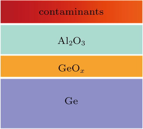
The gate-stack structure of the sample is shown in Fig. 1.

Fig. 1. (color online) The gate-stack structure of the sample.

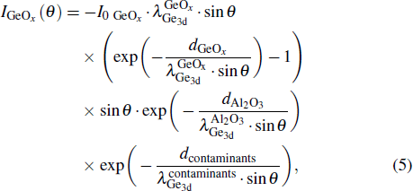
On the basis of the above discussion, the equations of measured intensity of Ge and GeOx are shown as follows:
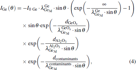
Here IGeOx(θ) and IGe(θ) is the areal intensity of GeOx and Ge, respectively, which is measured at the takeoff angle of θ. ρGeOx and ρGe is the germanium-atomic-density of GeOx and Ge of each atomic layer, respectively. dcontaminants, dAl2O3, and dGeOx are the thicknesses of contaminants, Al2O3, and GeOx, respectively. , , , and are the inelastic mean free path of photoelectrons of Ge 3d in GeOx, Ge, Al2O3, and contaminants, respectively. The items about Al2O3, contaminants, and any other material layer located upon the GeOx and Ge layers can be eliminated by dividing Eq. (4) from Eq. (5), because the intensity attenuation of Ge 3d of GeOx and Ge from such layers are the same. Then, the thickness of GeOx interface layer can be calculated by Eq. (6). The and are taken as 2.48 nm and 2.64 nm, respectively. The ρGeOx and ρGe are taken as 2.53 × 1022 cm−3 and 4.42 × 1022 cm−3.[47]

3. Results and discussion

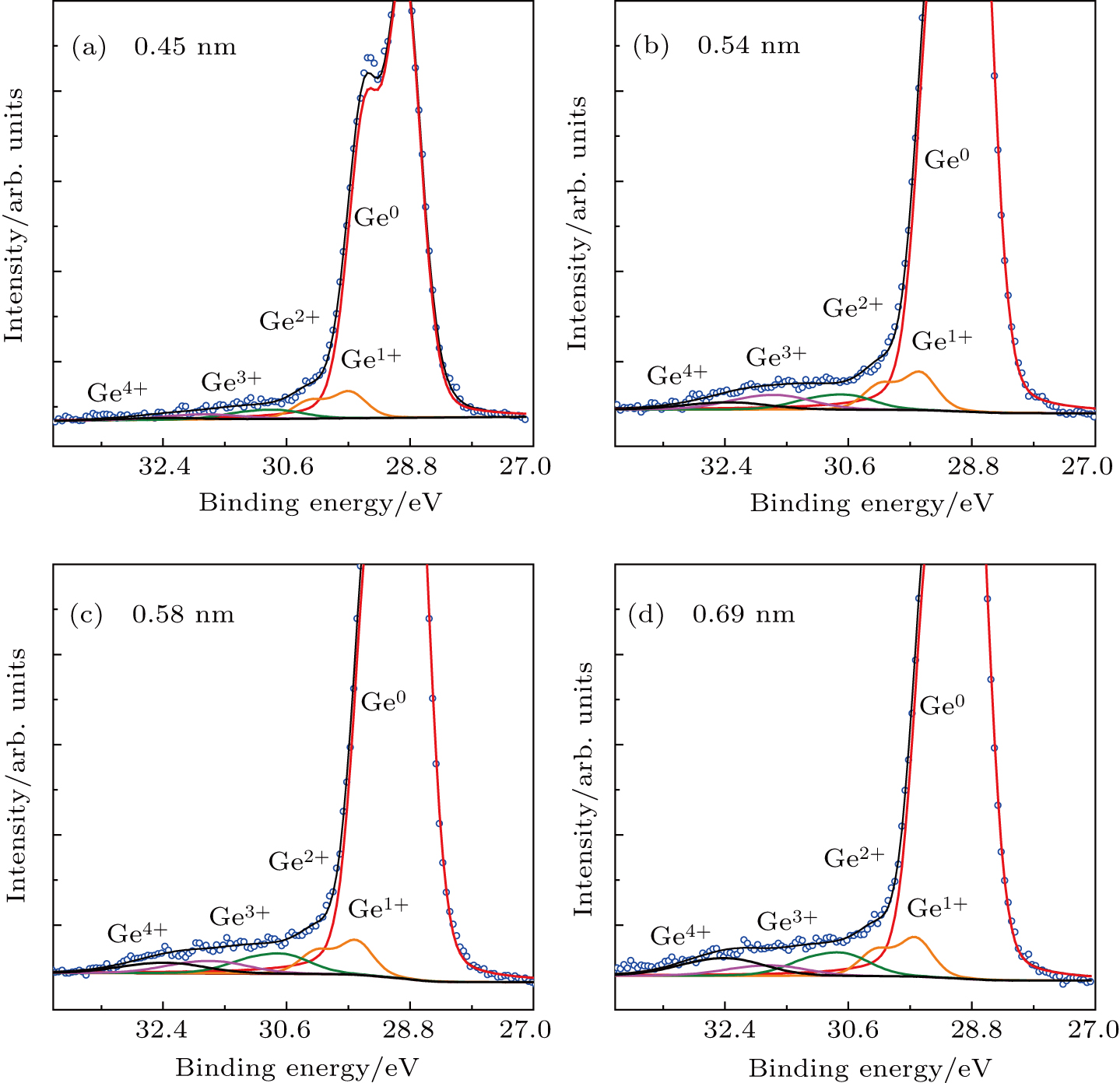
In order to investigate the oxidation states and their distributions in the GeOx interfacial layer formed by PPO, the XPS spectra of the Ge 3d core level were recorded and analyzed. Figure 2 shows the Ge 3d XPS spectra for Al2O3/GeOx/Ge structures with different GeOx thicknesses at a takeoff angle of 90°. In order to quantitatively estimate the various states of the Ge components, the Ge 3d spectra were deconvoluted into five peaks related to the Ge substrate (Ge0), Ge suboxide (Ge1+, Ge2+, and Ge3+), and GeO2 (Ge4+), as shown in Fig. 2. Further, the chemical shifts of Ge1+, Ge2+, Ge3+, and Ge4+ relative to Ge0 are taken as 0.8, 1.8, 2.75, and 3.4 eV, respectively.[48ȓ52] A spin–orbit splitting of 0.585 eV and a branching ratio of 2:3 are used for the 3d5/2 and Ge 3d3/2 doublets of the Ge 3d line shape. The Shirley background is used. The full width at half maximum (FWHM) is 0.57 eV for Ge0 and Ge1+, 0.9 eV for Ge2+, 1.12 eV for Ge3+, and 1.2 eV for Ge4+.[52] In addition, the symmetric Lorentzian–Gaussian convolution function is used, and the optimized percentage of the Lorentzian–Gaussian function is found to be 20%.

Fig. 2. (color online) Ge 3d XPS spectra for Al2O3/GeOx/Ge structures with different GeOx thicknesses at a takeoff angle of 90°. The Ge 3d spectra consist of five peaks related to the Ge substrate (Ge0), Ge suboxide (Ge1+, Ge2+, Ge3+), and GeO2 (Ge4+). The spin–orbit splitting of the Ge 3d5/2 and Ge 3d3/2 doublets is 0.585 eV.

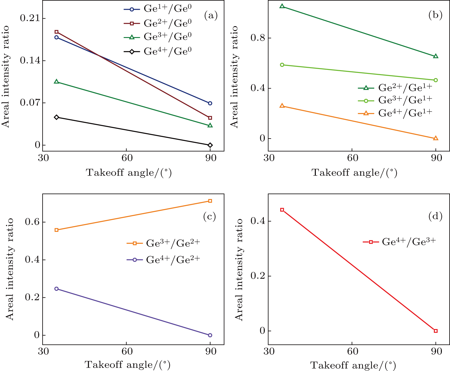
To obtain a better understanding of the oxidation process, it is necessary to clarify the depth distributions of the various oxidation states of Ge. Figure 3 shows the areal intensity ratios of the various states of Ge components as a function of the takeoff angle for a GeOx thickness of 0.59 nm after deconvolution of the spectra in Fig. 1. Considering that the spectra obtained with smaller takeoff angle are more sensitive to the surface, the photoelectrons received at a takeoff angle of 35° more often originate from the Ge atoms in the surface layer compared to those received at 90°. Therefore, the results measured at 35° are more likely to reflect the surface elements, whereas those measured at 90° reflect the elements in the entire sample.

Fig. 3. (color online) Areal intensity ratios of various states of Ge components as a function of the takeoff angle for a GeOx thickness of 0.59 nm. According to these results, the depth distributions of the Ge oxidation states are obtained.

It can be clearly observed from Fig. 3(a) that Gex+/Ge0 (x = 1, 2, 3, 4) decreases with increasing takeoff angle, suggesting that all oxidation states are located above the Ge0 states. A similar phenomenon is observed in Figs. 3(b), 3(c), and 3(d), indicating that the Gex+ (x = 2, 3, 4) states are located above the Ge1+ states, and the Ge4+ states appear above the Ge2+ and Ge3+ states. In contrast, the ratio of Ge3+/Ge2+ in Fig. 3(c) increases with increasing takeoff angle, demonstrating that the Ge2+ states are located above the Ge3+ states. On the basis of the above discussion, the distributions of the various oxidation states of Ge in 0.59-nm-thick GeOx are obtained as follows. The Ge4+, Ge2+, Ge3+, and Ge1+ states are localized from the GeOx surface to the GeOx/Ge interface but not in the order of Ge4+, Ge3+, Ge2+, and Ge1+ predicted by the layer-by-layer growth mode.[38]

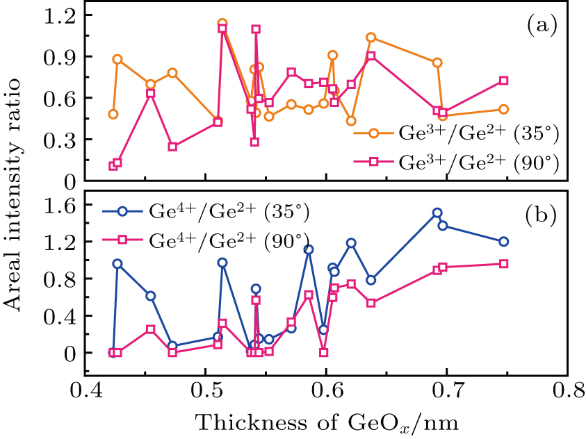
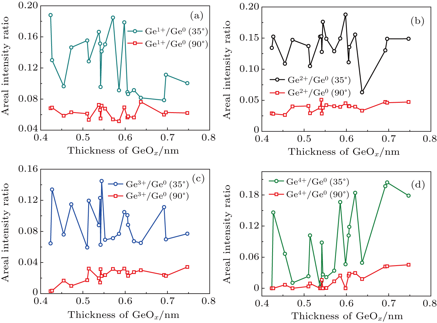
For a more objective understanding of the distributions of the Ge oxidation states during the oxidation process, the areal intensity ratios of various Ge oxidation states as a function of the GeOx thickness for takeoff angles of 35° and 90° have been investigated, as shown in Figs. 4, 5, and 6.
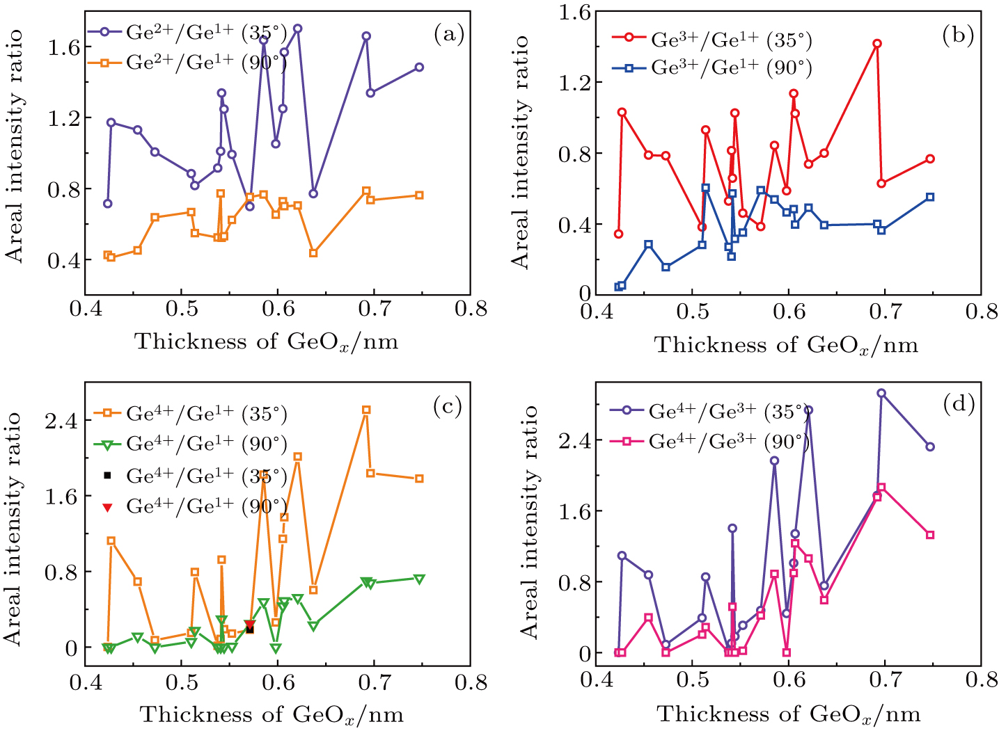
Fig. 4. (color online) Areal intensity ratios of Gex+/Ge0 (x = 1, 2, 3, 4) as a function of the GeOx thickness for takeoff angles of 35° and 90°. The relationship between the distributions of the Gex+ and Ge0 states can be acquired from these results.
Fig. 5. (color online) Areal intensity ratios of Gex+/Ge1+ (x = 2, 3, 4) and Ge4+/Ge3+ as a function of the GeOx thickness for takeoff angles of 35° and 90°.
Fig. 6. (color online) Areal intensity ratios of Ge3+/Ge2+ and Ge4+/Ge2+ as a function of the GeOx thickness for takeoff angles of 35° and 90°.

It can be clearly observed from Fig. 4 that the values of Gex+/Ge0 (x = 1, 2, 3, 4) at a takeoff angle of 35° are higher than those at 90° for GeOx thicknesses of 0.42–0.75 nm, suggesting that all Ge oxidation states are located above the Ge0 states. A similar phenomenon is observed for the results in Fig. 5, indicating that the Gex+ (x = 2, 3, 4) states are located above the Ge1+ states, and the Ge4+ states are located above the Ge3+ states. Figure 6 shows Ge3+/Ge2+ and Ge4+/Ge2+ as a function of the GeOx thickness. For Ge3+/Ge2+ in Fig. 6(a), Ge3+/Ge2+ for a takeoff angle of 90° is larger than that for 35° for some GeOx thicknesses and smaller for other GeOx thicknesses. These results indicate that the Ge2+ states appear above the Ge3+ states for some GeOx thicknesses and below the Ge3+ states for other GeOx thicknesses. Figure 6(b) shows Ge4+/Ge2+ as a function of the GeOx thickness. The Ge4+ states are located above the Ge2+ states. According to the discussion above, the distribution of the Ge oxidation states of the GeOx interfacial layer during the oxidation process are obtained as follows. The Ge4+ states, a mixture of Ge2+ and Ge3+ states, and the Ge1+ states are localized from the GeOx surface to the GeOx/Ge interface.

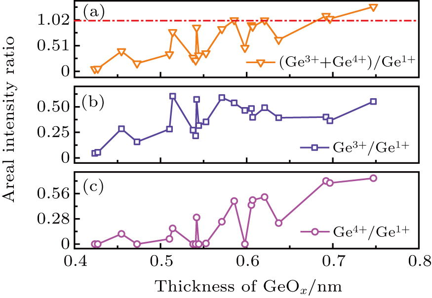
Figure 7 shows the areal intensity ratios of Gex+/Ge1+ (x = 3, 4) and (Ge3+ + Ge4+)/Ge1+ as a function of the GeOx thickness for a takeoff angle of 90°. It can be clearly observed that almost all areal intensity ratios (except for three) were less than 1.0, indicating that the number of Ge1+ states existing in a GeOx layer with a thickness of 1 nm or less is far greater than the numbers of Ge3+ and Ge4+ states and even greater than their sum. The Ge–Ge distance in GeO2 is in the range of 3.05 Å–3.15 Å,[53] which means that two layers of Ge should be oxidized for 0.7-nm-thick GeOx. Consequently, the Ge1+ states are predominant when the two outermost layers of Ge atoms are oxidized.

Fig. 7. (color online) Areal intensity ratios of Gex+/Ge1+ (x = 3, 4) and (Ge3+ + Ge4+)/Ge1+ as a function of the GeOx thickness for a takeoff angle of 90°.
4. Conclusions

In summary, the growth process of a GeOx film formed by PPO at RT is investigated on the basis of AR-XPS. In addition, the distributions of various Ge oxidation states are obtained by the areal intensity ratios of these states. It is experimentally found that the distributions of the Ge4+ states, a mixture of the Ge2+ and Ge3+ states, and the Ge1+ states are localized from the GeOx surface to the GeOx/Ge interface. Furthermore, the Ge1+ states are predominant when the two outermost layers of Ge atoms are oxidized. These experimental results are helpful for optimizing Ge-based gate stacks for future CMOSFET devices.

Reference
[1] Gupta S Gong X Zhang R Yeo Y C Takagi S Saraswat K C 2014 MRS Bull. 39 678
[2] Takagi S 2011 IEEE Int. Electron Devices Meeting Short course
[3] Xie Q Deng S Schaekers M Lin D Caymax M Delabie A Qu X P Jiang Y L Deduytsche D Detavernier C 2012 Semicond. Sci. Technol. 27 074012
[4] Saraswat K C Chui C O Krishnamohan T Nayfeh A McIntyre P 2005 Microelectron. Eng. 80 15
[5] Otani Y Itayama Y Tanaka T Fukuda Y Toyota H Ono T Mitsui M Nakagawa K 2007 Appl. Phys. Lett. 90 142114
[6] Maeda T Nishizawa M Morita Y Takagi S 2007 Appl. Phys. Lett. 90 072911
[7] Bera M K Mahata C Chakraborty A K Nandi S K Tiwari J N Hung J Y Maiti C K 2007 Semicond. Sci. Technol. 22 1352
[8] Sugawara T Oshima Y Sreenivasan R McIntyre P C 2007 Appl. Phys. Lett. 90 112912
[9] Ritenour A Hennessy J Antoniadis D A 2007 IEEE Electron Dev. Lett. 28 746
[10] Kim K H Gordon R G Ritenour A Antoniadis D A 2007 Appl. Phys. Lett. 90 212104
[11] Xie R Phung T H Yu M Zhu C 2010 IEEE Trans. Electron Dev. 57 1399
[12] Wu N Zhang Q Zhu C Chan D S H Li M F Balasubramanian N Chin A Kwong D L 2004 Appl. Phys. Lett. 85 4127
[13] Wu N Zhang Q Zhu C Chan D S H Du A Balasubramanian N Li M F Sin J K O Kwong D L 2004 IEEE Electron Dev. Lett. 25 631
[14] Caymax M Leys F Mitard J Martens K Yang L Pourtois G Vandervorst W Meuris M Loo R 2009 J. Electrochem. Soc. 156 H979
[15] Chen W B Shie B S Chin A 2011 IEEE Electron Dev. Lett. 32 449
[16] Frank M M Koester S J Copel M Ott J A Loesing R 2006 Appl. Phys. Lett. 89 112905
[17] Xie R Zhu C 2007 IEEE Electron Dev. Lett. 28 976
[18] Sioncke S Lin H C Brammertz G Delabie A Conard T Franquet A Meuris M Struyf H De Gendt S Heyns M Fleischmann C Temst K Vantomme A Müller M Kolbe M Beckhoff B Caymax M 2011 J. Electrochem. Soc. 158 H687
[19] Merckling C Chang Y C Lu C Y Penaud J El-Kazzi M Bellenger F Brammertz G Hong M Kwo J Meuris M Dekoster J Heyns M M Caymax M 2011 Microelectron. Eng. 88 399
[20] Matsubara H Sasada T Takenaka M Takagi S 2008 Appl. Phys. Lett. 93 032104
[21] Hosoi T Kutsuki K Okamoto G Saito M Shimura T Watanabe H 2009 Appl. Phys. Lett. 94 202112
[22] Lee C H Tabata T Nishimura T Nagashio K Kita K Toriumi A 2009 Appl. Phys. Express 2 071404
[23] Lee C H Nishimura T Nagashio K Kita K Toriumi A 2011 IEEE Trans. Electron Dev. 58 1295
[24] Delabie A Bellenger F Houssa M Conard T Elshocht S V Caymax M Heyns M Meuris M 2007 Appl. Phys. Lett. 91 082904
[25] Matsubara H Sasada T Takenaka M Takagi S 2008 Appl. Phys. Lett. 93 032104
[26] Xie R He W Yu M Zhu C 2008 Appl. Phys. Lett. 93 073504
[27] Gu J J Liu Y Q Xu M Celler G K Gordon R G Ye P D 2010 Appl. Phys. Lett. 97 012106
[28] Delabie A Alian A Bellenger F Caymax M Conard T Franquet A Sioncke S Van Elshocht S Heyns M M Meuris M 2009 J. Electrochem. Soc. 156 G163
[29] Kuzum D Krishnamohan T Pethe A J Okyay A K Oshima Y Sun Y McVittie J P Pianetta P A McIntyre P C Saraswat K C 2008 IEEE Electron Dev. Lett. 29 328
[30] Yang X Wang S K Zhang X Sun B Zhao W Chang H D Zeng Z H Liu H 2014 Appl. Phys. Lett. 105 092101
[31] Wang X L Xiang J J Wang W W Xiong Y H Zhang J Zhao C 2015 Appl. Surf. Sci. 357 1857
[32] Fukuda Y Yazaki Y Otani Y Sato T Toyota H Ono T 2010 IEEE Trans. Electron Dev. 57 282
[33] Zhang R Iwasaki T Taoka N Takenaka M Takagi S 2012 IEEE Trans. Electron Dev. 59 335
[34] Takenaka M Zhang R Takagi S 2013 Reliability Physics Symposium IRPS 4C.1.1 4C.1.8
[35] Takagi S Zhang R Takenaka M 2013 Microelectron. Eng. 109 389
[36] Zhang R Lin J C Yu X Takenaka M Takagi S 2013 Microelectron. Eng. 109 97
[37] Zhang R Huang P C Lin J C Takenaka M Takagi S 2013 Appl. Phys. Lett. 102 081603
[38] Zhang R Huang P C Lin J C Taoka N Takenaka M Takagi S 2013 IEEE Trans. Electron Dev. 60 927
[39] Takahashi T Nishimura T Chen L Sakata S Kita K Toriumi A 2007 IEEE Int. Electron Devices Meeting 697
[40] Hattori T Suzuki T 1983 Appl. Phys. Lett. 43 470
[41] Zhang R Chern W Yu X Takenaka M Hoyt J L Takagi S 2013 IEEE Int. Electron Devices Meeting 26.1.1 26.1.4
[42] Zhang R Lin J C Yu X Takenaka M Takagi S 2013 Symp. VLSI Technology T26 T27
[43] Zhang R Huang P C Lin J C Takenaka M Takagi S 2012 IEEE Int. Electron Devices Meeting 371 374
[44] Hosoi T Kutsuki K Okamoto G Saito M Shimura T Watanabe H 2009 Appl. Phys. Lett. 94 202112
[45] Ogawa S Suda T Yamamoto T Kutsuki K Hideshima I Hosoi T Shimura T Watanabe H 2011 Appl. Phys. Lett. 99 142101
[46] Fukuda Y Ueno T Hirono S Hashimoto S 2005 Jpn. J. Appl. Phys. 44 6981
[47] Kimihiko K Kyogoku S Sakashita M Takeuchi W Kondo H Takeuchi S Nakatsuka O Zaima S 2011 Jpn. J. Appl. Phys. 50 10
[48] Sun S Sun Y Liu Z Lee D I Pianetta P 2006 Appl. Phys. Lett. 89 231925
[49] Renault O Fourdrinier L Martinez E Clavelier L Leroyer C Barrett N Crotti C 2007 Appl. Phys. Lett. 90 052112
[50] Kato K Kyogoku S Sakashita M Takeuchi W Kondo H Takeuchi S Nakatsuka O Zaima S 2011 Jpn. J. Appl. Phys. 50 10PE02
[51] Sahari S K Murakami H Fujioka T Bando T Ohta A Makihara K Higashi S Miyazaki S 2011 J. Appl. Phys. 50 04DA12
[52] Wang X L Zhao Z Q Xiang J J Wang W W Zhang J Zhao C Ye T C 2016 Appl. Surf. Sci. 390 472
[53] Glinnemann J King H E Jr Schulz H Hahn Th La Placa S J Dacol F 1992 Z. Kristall. – Cryst. Mater. 198 177