† Corresponding author. E-mail:
Graphene-based heterostructure is one of the most attractive topics in physics and material sciences due to its intriguing properties and applications. We report the one-step fabrication of a novel graphene/Mo2C heterostructure by using chemical vapor deposition (CVD). The composition and structure of the heterostructure are characterized through energy-dispersive spectrometer, transmission electron microscope, and Raman spectrum. The growth rule analysis of the results shows the flow rate of methane is a main factor in preparing the graphene/Mo2C heterostructure. A schematic diagram of the growth process is also established. Transport measurements are performed to study the superconductivity of the heterostructure which has potential applications in superconducting devices.
Since the discovery of graphene in 2004,[1–4] many new two-dimensional (2D) materials have been found,[5–8] and 2D ultrathin Mo2C is one of them.[9,10] Mo2C belongs to the transition metal carbide, which combines the characteristics of ceramics and metals.[11,12] Mo2C has not only high strength and hardness but also excellent catalytic activity and superconducting properties.[13] Scientists have fabricated large-area high-quality 2D ultrathin α-Mo2C. The research of its physical properties, such as superconductivity and magnetotransport properties,[9,14] have achieved an important breakthrough.
Contemporarily, an important development trend in 2D material research field is the extension from a single material to an artificial heterostructure formed by two materials.[15–19] In the heterostructure, the superlattice periodic potential field caused by lattice mismatch exhibits a significant modulating action on the energy band structure of 2D materials. Moreover, it presents a novel quantum phenomenon which is not observed in single material.[20–23] Superconducting materials and graphene heterostructures, such as graphene/Bi2Sr2CaCu2O8+x heterostructure, show an obvious nonlinear I–V characteristic, which indicates a possibility for developing the new superconducting devices.[24] Traditional 2D heterostructures are mainly prepared through a two-step process. This process includes either growing two materials in different conditions and then combining them to form a heterostructure, or growing one material directly onto another which is prepared as a substrate (epitaxial growth). Such a complicated preparation process tends to introduce contaminations at the interface and therefore has some limitations.
In this work, the graphene/ultrathin Mo2C heterostructure is fabricated for the first time by one-step chemical vapor deposition (CVD) process, which can effectively avoid contaminations introduced in the traditional two-step growth process of heterostructure. The structure of heterostructure is verified. The key factor in fabricating the graphene/Mo2C heterostructure and growth process is studied. The transport properties of the heterostructure are also measured.
Cu (99.8% purity, 100-μm thick)/Mo (99.8% purity, 100-μm thick) foil as substrate were placed in a horizontal quartz tube furnace. Then, the samples were annealed under a flow of Ar/H2 (5:1) at 1000 °C before growth to remove surface contamination. Subsequently, mixed methane, hydrogen, and argon gas were fed into the reaction chamber at different flow rates, with the temperature kept at 1086 °C. Upon the synthesis of heterostructure, the samples were then cooled down to room temperate naturally.
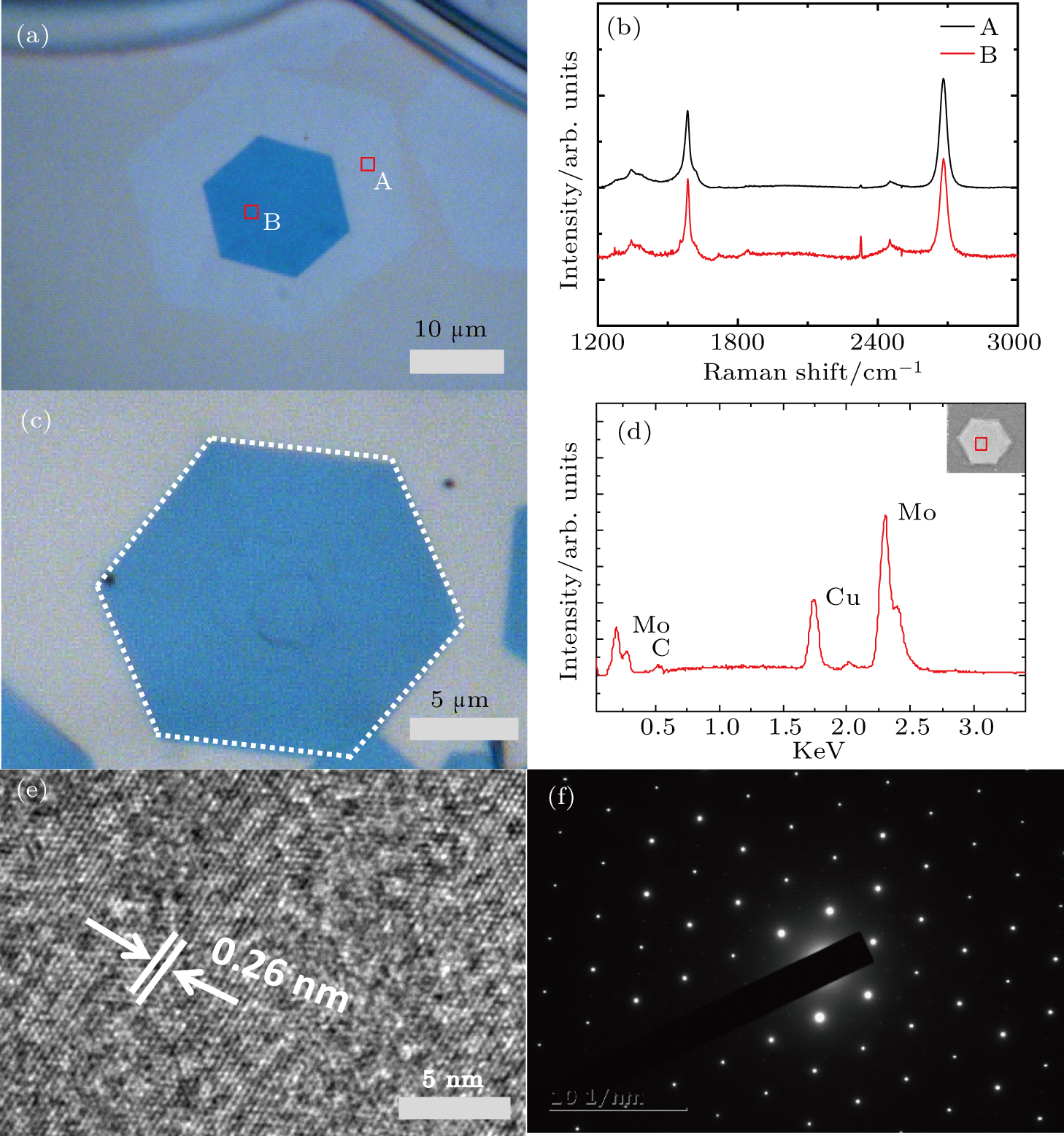
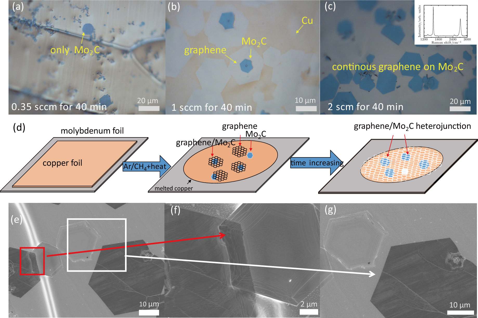
Graphene/Mo2C heterostructure can be fabricated using CVD under the following growth condition: 1-sccm CH4, 200-sccm H2, 1000-sccm Ar, 40 min, 100-μm Cu above 100-μm Mo. Figure
We then confirm the structure of Mo2C through several methods. Figure
Figure
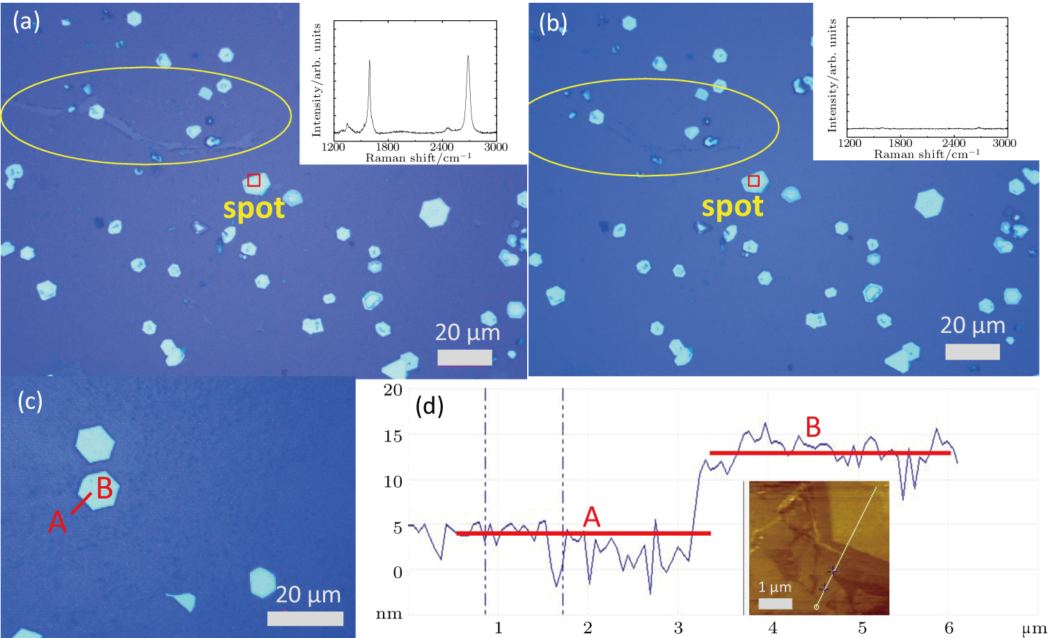
Figure
The resulting heterostructures are transferred onto SiO2/Si (300 nm/500 μm) substrates for characterization and application using a polymethylmethacrylate-supported transfer method.[25–27] Figure
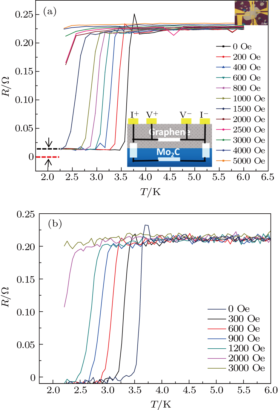
Four-point probe measurement is performed on each of the graphene/Mo2C heterostructure samples at the temperatures ranging from 2 K to 6 K by Physical Property Measurement System (PPMS, Quantum Design). Optical image of the device for transport measurement is shown in the inset of Fig.
In the present study, we successfully fabricate vertical graphene/Mo2C heterostructure by using CVD directly. We summarize the growth rule of the heterostructure and find that Mo2C crystals and graphene can be simultaneously grown with the high flow rate of methane and have the potential to form heterostructures. A schematic diagram of the growth process is also established. Finally, we study the superconductivity of the heterostructure after successfully transferring it onto Si2O/Si substrate.
| [1] | |
| [2] | |
| [3] | |
| [4] | |
| [5] | |
| [6] | |
| [7] | |
| [8] | |
| [9] | |
| [10] | |
| [11] | |
| [12] | |
| [13] | |
| [14] | |
| [15] | |
| [16] | |
| [17] | |
| [18] | |
| [19] | |
| [20] | |
| [21] | |
| [22] | |
| [23] | |
| [24] | |
| [25] | |
| [26] | |
| [27] |


