Graphene/Mo2C heterostructure directly grown by chemical vapor deposition
Project supported by the National Natural Science Foundation of China (Grant Nos. 1402342, 11574338, and 11274333), the Hundred Talents Program of Chinese Academy of Sciences, the International Collaboration and Innovation Program on High Mobility Materials Engineering, Chinese Academy of Sciences (Grant No. KGZD-EW-303), and the "Strategic Priority Research Program (B)" of the Chinese Academy of Sciences (Grant No. XDB04040300).
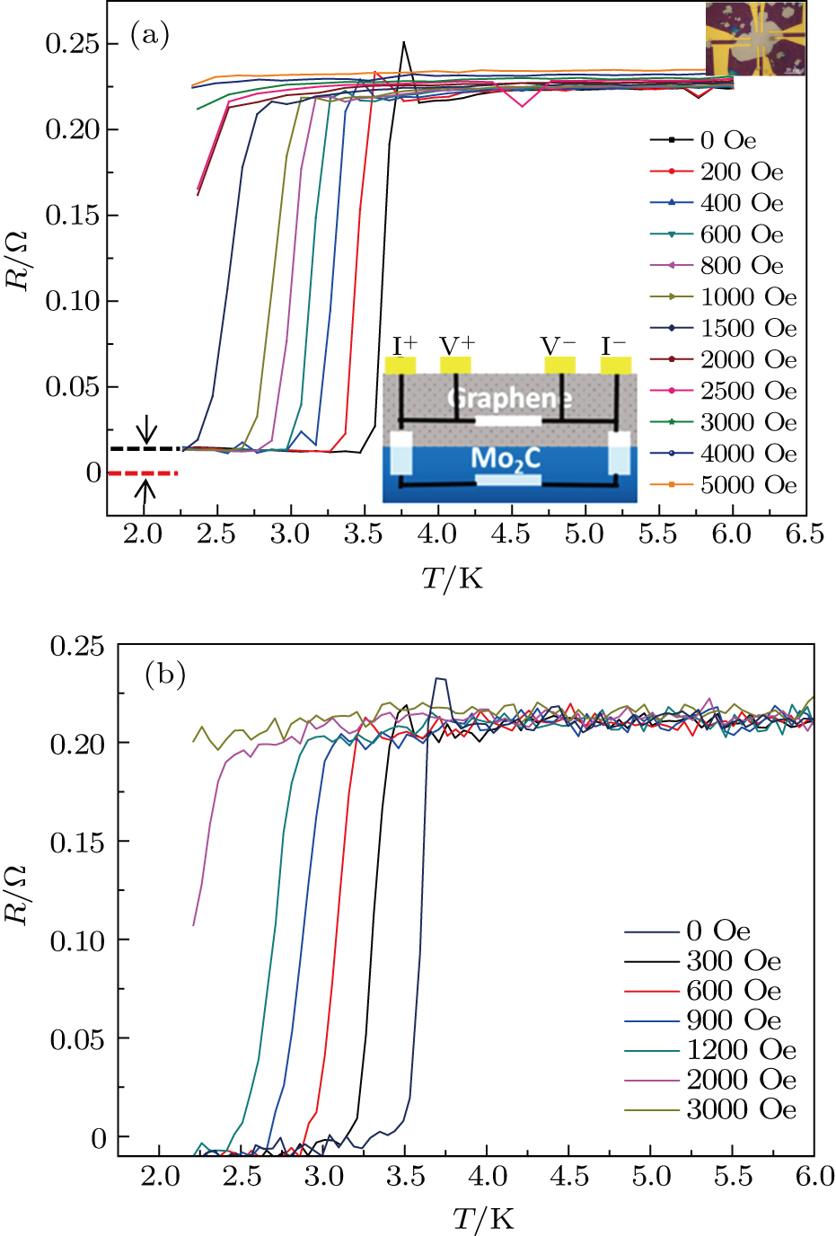
(color online) Typical temperature dependence of resistance of graphene/Mo2C heterostructure under various magnetic fields before (a) and after oxygen plasma etching (b). Inset in panel (a) shows an optical image of the device for transport measurement (upper left corner) and a brief circuit diagram of the transport measurement in the middle. The unit 1 Oe = 79.5775 A⋅m−1.