Graphene/Mo2C heterostructure directly grown by chemical vapor deposition
Project supported by the National Natural Science Foundation of China (Grant Nos. 1402342, 11574338, and 11274333), the Hundred Talents Program of Chinese Academy of Sciences, the International Collaboration and Innovation Program on High Mobility Materials Engineering, Chinese Academy of Sciences (Grant No. KGZD-EW-303), and the "Strategic Priority Research Program (B)" of the Chinese Academy of Sciences (Grant No. XDB04040300).
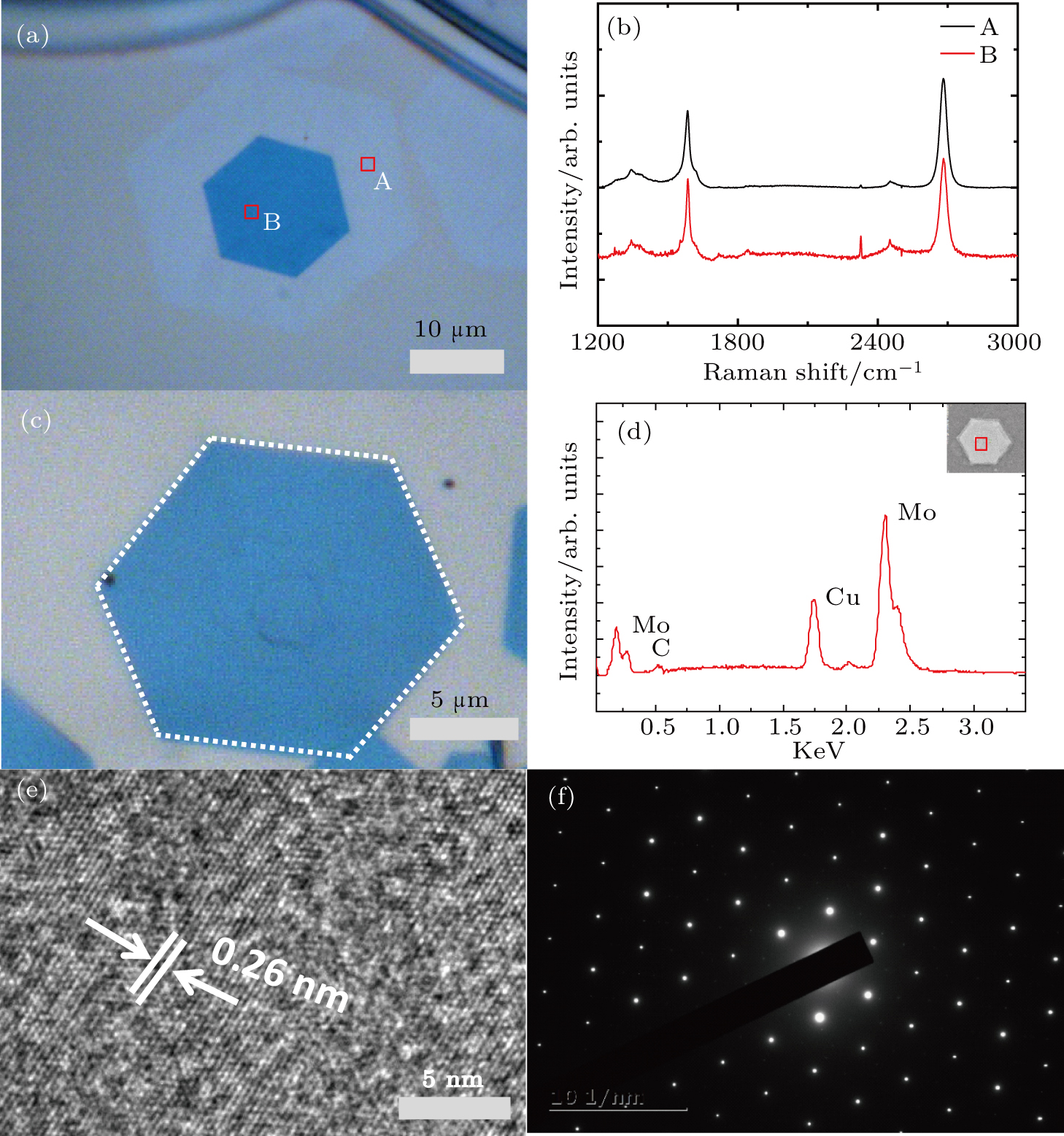
(color online) (a) OM image of Mo2C/graphene heterostructure. (b) Raman spectra of A and B, respectively. (c) Optical image and (d) typical EDS image spectrum of Mo2C crystal fabricated by using CVD under the following condition: 1-sccm CH4, 200-sccm H2, 1000-sccm Ar, 40 min, and 100-μm Cu above 100-μm Mo. (e) HRTEM image and (f) SAED pattern of Mo2C crystal. The inset in panel (d) shows the corresponding Mo2C crystal (the same as those shown in panel (c)), and the red spot shows the position where the EDS spectrum is acquired.