Strain engineering of electronic and magnetic properties of Ga2S2 nanoribbons
Wang Bao-Ji1, Li Xiao-Hua1, Zhang Li-Wei1, Wang Guo-Dong1, Ke San-Huang2, †
School of Physics and Electronic Information Engineering, Henan Polytechnic University, Jiaozuo 454000, China
MOE Key Labortoray of Microstructured Materials, School of Physics Science and Engineering, Tongji University, Shanghai 200092, China


† Corresponding author. E-mail: shke@tongji.edu.cn

Abstract

Using first-principles calculations, we study the tailoring of the electronic and magnetic properties of gallium sulfide nanoribbons (Ga2S2NRs) by mechanical strain. Hydrogen-passivated armchair- and zigzag-edged NRs (ANRs and ZNRs) with different widths are investigated. Significant effects in band gap and magnetic properties are found and analyzed. First, the band gaps and their nature of ANRs can be largely tailored by a strain. The band gaps can be markedly reduced, and show an indirect-direct (I-D) transition under a tensile strain. While under an increasing compressive strain, they undergo a series transitions of I-D-I-D. Five strain zones with distinct band structures and their boundaries are identified. In addition, the carrier effective masses of ANRs are also tunable by the strain, showing jumps at the boundaries. Second, the magnetic moments of (ferromagnetic) ZNRs show jumps under an increasing compressive strain due to spin density redistribution, but are unresponsive to tensile strains. The rich tunable properties by stain suggest potential applications of Ga2S2NRs in nanoelectronics and optoelectronics.

1. Introduction

Since the successful exfoliation of graphene, two-dimensional (2D) nanomaterials, such as boron nitride,[1,2] molybdenum disulfide (MoS2),[3] and others,[46] have attracted a great deal of attention due to their interesting physical and chemical properties. Recently, monolayer Ga2S2, as a new kind of metal chalcogenide material with a 2D honeycomb structure, was fabricated by mechanical exfoliation from the bulk, and was also successfully grown in 2D and quasi-1D forms by vapor transport techniques.[4,7,8] The Ga2S2 monolayer consists of S–Ga–Ga–S atomic layers with a Ga–Ga dimer covalently bonded to six S atoms, leading to a symmetry of and an in-plane lattice constant of 3.587 Å. Its structural and electronic properties have been studied by density functional theory (DFT) calculations. For instance, Zólyomi et al. demonstrated that the Ga2S2 monolayer is dynamically stable and is an indirect-band-gap semiconductor with an unusual inverted sombrero dispersion near the top of the valence band.[9] Zhuang et al. predicted that Ga2S2 structures are suitable for photocatalytic water splitting by performing hybrid DFT and quasi-particle calculations.[10] Similar to the case of graphene, the Ga2S2 monolayer can also be cut into nanoribbons (Ga2S2NRs) with two typical shapes of edge: zigzag and armchair. The different edge chiralities lead to distinct electronic and magnetic properties: zigzag nanoribbons (ZGa2S2NRs) are ferromagnetic (FM) and metallic regardless of H-passivation, while armchair ones (AGa2S2NRs) are nonmagnetic (NM) semiconductors.[11,12]

Tunability of electronic and magnetic properties of a material by external controls, such as strain, is very beneficial for its applications in nanoelectronics and optoelectronics.[1315] Recently, it was found that the band gap of Ga2S2 monolayer decreases near linearly with increasing tensile strain, and the effective mass of carrier exhibits a strong anisotropy and can also be effectively modulated by applying a compressive or tensile strain.[16,17] Orudzhev et al. showed that the elastic constants of the GaS layered compound increase monotonically with increasing pressure in the range of 0–20 GPa.[18] A theoretical study demonstrated that the electronic properties of GaS/GaSe heterostructures can be continuously tuned by an external strain.[19] These findings suggest that strain engineering is a simple and promising way to modulate the intrinsic physical properties of low-dimensional nanomaterials. Therefore, one may ask, what are the effects of external strains on Ga2S2NRs? How can significant modulation of their electronic and magnetic properties be achieved by applying strains? To date, the answers have not been available in the literature to the best of our knowledge.

In this work, we investigate the strain modulation of electronic and magnetic properties of Ga2S2NRs by performing first-principles DFT calculations. The elastic limits of Ga2S2NRs are firstly examined in terms of stress–strain relations. For nonmagnetic and semiconducting AGa2S2NRs within the elastic limit, the shifts of the band edges and the nature of the band gaps are investigated by analyzing the evolution of the band structure under different strains. Several critical strains are found to trigger an indirect-direct (I-D) transition. This detailed knowledge about the band gap I-D transition can be very useful for the optical applications of AGa2S2NRs. For example, a similar strain-induced I-D transition in GaAs nanowires was predicted theoretically[20,21] and observed in a recent experiment,[22] in which the luminescence of the GaAs nanowires can be switched on and off by changing the uniaxial stress applied. Besides the band gap modulation, the electron and hole effective masses in AGa2S2NRs are also found to be tunable by the strain. For ferromagnetic and metallic ZGa2S2NRs, we focus on the strain modulation of the magnetic moments.

2. Structure modeling and computational details

The structures of Ga2S2NRs are initially constructed by cutting out a stripe of Ga2S2 sheet with the desired edges and widths. Following the previous convention,[2325] the number of dimer lines (An) or zigzag chains (Zn) across the ribbon width is used to present the width of an armchair-edged ribbon (henceforth denoted as An-Ga2S2NR) (see Fig. 1(a)) or a zigzag-edged ribbon (denoted as Zn-Ga2S2NR) (see Fig. 1(b)). All edge atoms are passivated by hydrogen atoms to eliminate the dangling bonds. A strain is applied by changing the lattice constant along the periodic direction, , with a and being the deformed and the equilibrium lattice constants, respectively. Positive values of refer to expansion, while negative values correspond to compression. Under each strain condition, all atoms are fully relaxed, whereas the lattice constant is fixed.

Fig. 1. (color online) Top and side views of the atomic structures of Ga2S2NRs with hydrogen-passivated armchair (a) and zigzag (b) edges.

The atomic structure relaxation and electronic structure calculations are carried out in Kohn–Sham DFT as implemented in the Vienna ab initio simulation package (VASP).[26] The projector augmented wave method (PAW)[27] is used to describe the ion–electron interaction. Plane waves with a kinetic energy cutoff of 600 eV are used to expand the wave functions. The electron exchange and correlation are treated by the generalized gradient approximation (GGA)[28] in the version of Perdew–Burke–Ernzerhof (PBE).[29] The 4s24p1 electrons of Ga and 3s23p4 electrons of S are treated as the valence electrons. Periodic boundary conditions (PBC) are employed for the infinitely long nanoribbon systems and a vacuum space of 15 Å in each direction perpendicular to the ribbon is used to eliminate the interactions between the periodic images. The atomic structures of the systems are relaxed with the conjugate gradient method until the force on each atom is less than 0.01 eV/Å. For the structure optimization, a Monkhorst–Packs k-mesh of 1 × 1 × 21 is used for the Brillouin zone (BZ) sampling. The band structures are presented by 45 k points. The results for free-standing Ga2S2NRs given by the present computational parameters are consistent with those in the previous calculations.[12]

3. Results and discussion
3.1. Stress–strain relations and elastic limits of Ga2S2NRs

Generally, the elastic limit of a crystal is defined as the sustainable maximum strain under tension or compression. When the strain of the crystal is larger than the elastic limit, the deformation of the crystal is irreversible, which is called mechanical failure. In order to estimate the elastic limits of Ga2S2NRs, we first calculate the stress (force) of Ga2S2NRs as a function of strain by using the method described in Refs. [30] and [31], which was originally proposed for three-dimensional crystals. Considering that the thickness of a Ga2S2NR is not well defined, we present the stress using force instead of force per unit area.[32] For AGa2S2NRs, four widths (An, n = 4, 5, 12, and 13) are considered, while for ZGa2S2NRs, which are all metallic regardless of the ribbon width, only one width (Z6-Ga2S2NR) is considered. The calculated stress–strain relations are presented in Fig. 2. It shows that for small strains (∼ −8% to +8%) the stress in AGa2S2NRs responds near linearly to the strain, while for larger strains, it responds nonlinearly. For a fixed strain, the stress increases with the increasing ribbon width; this is simply due to the use of force instead of force per unit area. Based on the results in Fig. 2 we can determine the elastic limit which corresponds to the maximum stress in each curve. The results for the four AGa2S2NRs are −20%, −19%, −18%, and −19%, respectively, for compressive strain, and +22%, +19%, +19%, and +20%, respectively, for tensile strain. For Z6-Ga2S2NR (see the inset in Fig. 2), the stress–strain relation is nonlinear and the strain limits are −22% and +26% for compressive and tensile strains, respectively. We note that, similar to the mechanical properties of graphene nanoribbons (GNRs),[24,33,34] the elastic limit of ZGa2S2NRs is larger than that of AGa2S2NRs, and the values are close to those of other quasi-1D materials, such as GNRs[24,33,34] and silicene nanoribbons.[35]

Fig. 2. (color online) Stress–strain relations for AGa2S2NRs with different widths under strains. The inset shows a similar relation for Z6-Ga2S2NR.
3.2. Strain effects on electronic properties of armchair nanoribbons

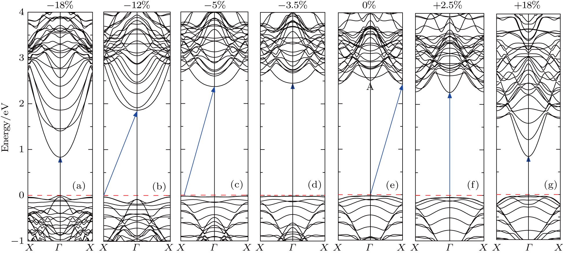
Our calculations show that the AGa2S2NRs with different widths undergo a series of band gap I-D transitions under an increasing strain from −18% to +18%. As an example, the band structures of A13-Ga2S2NR under various strains are given in Fig. 3 with the strains labelled. Under zero strain, the free-standing A13-Ga2S2NR possesses an indirect band gap between the conduction band minimum (CBM) at X and the valence band maximum (VBM) at Γ (see Fig. 3(e)). Under a tensile strain up to +18%, the VBM remains at Γ, while the conduction band bottom at Γ (denoted by A in Fig. 3(e)) shifts down rapidly, leading to a direct band gap at Γ for ε >+2.3% (see Figs. 3(f) and 3(g)). We note that such a shift of the A state under strains is a result of the competition of the different electronic orbitals near the CBM. In Fig. A1 (see Appendix A), we show the calculated total and partial densities of states (PDOSs) of A13-Ga2S2NR under the different strains. As one can see in Fig. A1(b), the states around the CBM of the unstrained A13-Ga2S2NR are dominated by the 3pz orbitals of S atoms and 4p orbitals of Ga atoms. The in-plane p orbitals with -like states are generally more sensitive to the in-layer strain than the out-of-plane pz orbitals with -like states.[36] Consequently, in the CBM of the stretched A13-Ga2S2NR, the Ga 4p orbitals are gradually decreased while the s orbitals of Ga atoms evolve into the preponderant states, leading to the down-shift of the CBM, as can be seen in Fig. A1(a). Meanwhile, the 3pz orbitals of S atoms are unresponsive to the in-layer strain and thus stay nearly the same. The similar behavior is found in the compression cases, as shown in Fig. A1(c). When an increasing compressive strain (up to −18%) is applied, the A state also shifts down rapidly and the CBM is kept at Γ for ε < −1.7%, while the VBM appears alternately at Γ and X, leading to a series of I-D-I-D transitions (see Figs. 3(e)3(a)). The strains of −1.7% and +2.3% are the two critical strains under which the conduction band bottoms at Γ and X are equal. This behavior would have potential applications for valleytronic devices: quasiparticles with the same energy at different positions in the momentum space are less susceptible to phonon scattering.[37,38]

Fig. 3. (color online) Strain-induced indirect-direct band gap transition in A13-Ga2S2NR. The arrows are from VBM to CBM.

We note that the Kohn–Sham DFT calculations usually underestimate band gaps of semiconductors because of the lacking of the derivative discontinuity in the energy functionals. However, the shapes of the frontier valence band and conduction band are usually reliable and are close to the result from many-body quasi-particle calculations. Our work here is focused on the trend in the band gap variation under different strains instead of the absolute values of the band gap, therefore the results can be expected to be meaningful. This justification is also supported by the previous calculations using the hybrid functional HSE06 and PBE, showing consistent strain-induced effects on the band structures.[39]

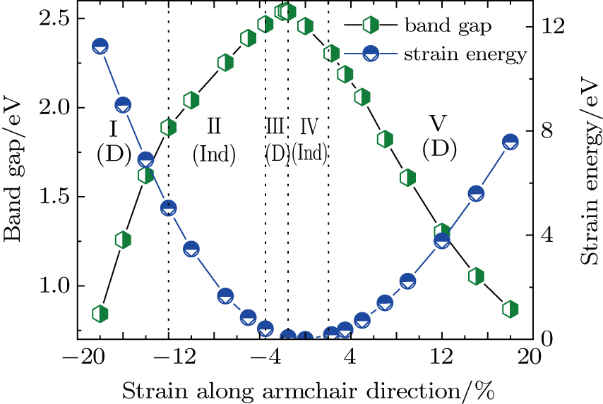
In Fig. 4, we summarize the band gap and the strain energy of A13-Ga2S2NR as functions of the strain applied, together with the five strain zones (I, II, III, IV, and V) identified based on the distinct band structures. The five zones correspond to the D-I-D-I-D band gap transitions, with the boundaries located at −12%, −3.5%, −1.7%, and +2.3%, respectively, as indicated by the dotted lines in Fig. 4. One can see that the band gap reaches its maximum value (∼ 2.5 eV) at the strain of about −1.7% and then decreases with the compressive or tensile strain increasing. At the maximum tensile and compressive strains (±18%), the band gap decreases to 0.87 eV and 0.84 eV, respectively.

Fig. 4. (color online) Band gap and strain energy of A13-Ga2S2NR as functions of the strain applied. Five strain zones (I, II, III, IV, and V) are identified based on the distinct band structures, which correspond to the D-I-D-I-D band gap transitions. The critical strains for the transitions are −12%, −3.5%, −1.7%, and +2.3%, respectively, as indicated by the dotted lines.
3.3. Strain effects on the carrier effective mass of armchair nanoribbons

The effective masses of electron and hole in the ribbon direction are determined by , where E and k correspond to the energy and the reciprocal lattice vector along the nanoribbon. The results are related to the shapes of the energy bands around the CBM and VBM, respectively. The significant effects of the strain on the CBM and VBM will also affect and , especially the switches of CBM or VBM between Γ and X. In Fig. 5, we plot and in units of free electron mass ( ) as functions of strain for A13-Ga2S2NR. Under zero strain, the electron effective mass ( ) is much less than the hole effective mass ( ). Under strains, the electron effective mass shows small or large jumps at the strain zone boundaries and is approximately a constant within each zone (plateaus structure). This is due to the change in the CBM nature: the jump around −12% strain is caused by the change of CBM from a fat conduction band to a slim one; the other three are related to the switches of CBM between Γ and X. On the other hand, the variation of the hole effective mass is much larger and does not show the plateaus structure. It reaches its maximum ( ) at −3.5% strain and then decreases with the increasing compressive or tensile strain except for very large strains (> ∼ ±14%). The much larger for small strains is due to the very flat frontier valence band which makes the Γ-X switch of the VBM not so remarkable, thus making the plateaus structure absent. Overall, the electron and hole effective masses in A13-Ga2S2NR will be decreased by applying moderate tensile strains, as shown in Fig. 5, which would be beneficial for applications in nanoelectronics.

Fig. 5. (color online) Hole and electron effective masses as functions of strain for A13-Ga2S2NR.
3.4. Strain effects on magnetic properties of zigzag nanoribbons

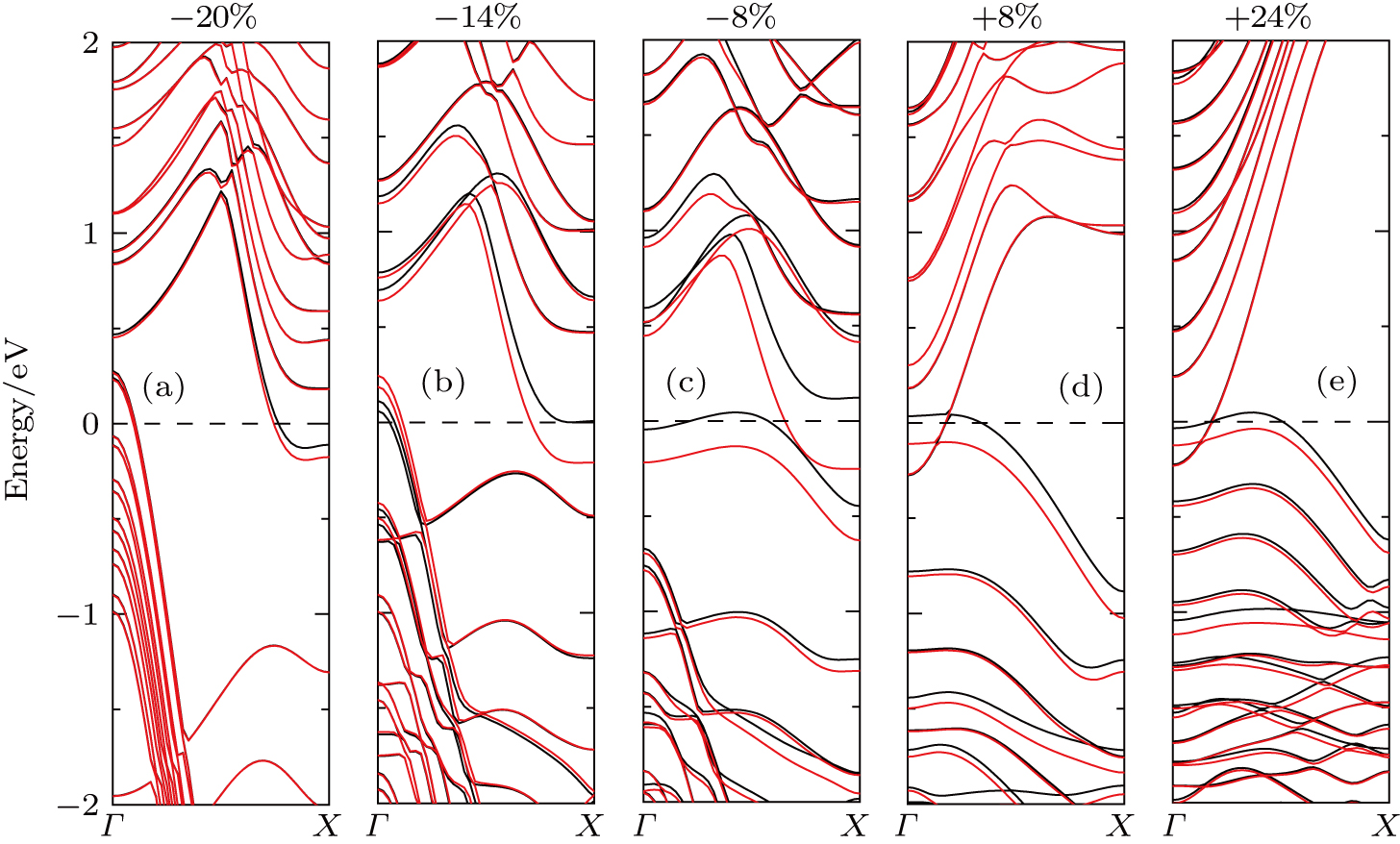
The present calculations and a previous work[12] show that ZGa2S2NRs are ferromagnetic and metallic. Here we investigate the strain effects on the magnetic properties of ZGa2S2NRs by taking Z6-Ga2S2NR as an example. Strains ranging from −20% to +24% are considered. The calculated band structures under various strains (Fig. 6) show that the strained ribbon is still metallic and magnetic. For moderate strains (−14% to +8%), the spin polarization occurs mainly around the Fermi energy, while for very large compressive strains (around −20%), the spin-up and spin-down band structures become very close to each other, indicating that the spin polarization and the FM stability are weakened. To check the stability of the FM phase under strains, we calculate the energy difference between the NM and FM phases, , and plot the result as a function of strain in Fig. 7(a) together with the strain energy. One can see that decreases slowly from 8.77 meV to 4.13 meV with the tensile strain increasing from zero to +24%, indicating that the tensile strains will weaken the FM stability. However, when an increasing compressive strain is applied, first increases sharply to its maximum (32.35 meV at the strain of −2%) and then decreases gradually to zero. A moderate compressive strain in the range from −2% to −12% will enhance the FM stability with respect to the NM phase. When the compressive strain is larger than −14%, however, the total magnetic moment is largely suppressed and the system eventually becomes antiferromagnetic (AFM) as discussed later.

Fig. 6. (color online) Calculated band structures of Z6-Ga2S2NRs under various strains: (a) −20%, (b) −14%, (c) −8%, (d) +8%, and (e) +24%. Red and black lines are for spin-up and spin-down states, respectively.
Fig. 7. (color online) (a) Energy difference between the NM and FM phases and the strain energy of Z6-Ga2S2NR as functions of strain. Note that for strains higher than −12%, the system is in a mixed FM and AFM state. (b) Strain-dependent magnetic moment of Z6-Ga2S2NR. The results for strains higher than −14% are not shown because the magnetic state is not favorable. The insets show the spin distributions under the strains indicated.

Next let us look at the strain effects on the magnetic moment, as shown in Fig. 7(b). The magnetic moment per cell in Z6-Ga2S2NR is nearly unresponsive to a tensile strain up to +24%. This is different from the case of MoS2 nanoribbons, where the tensile strains produce a reversible modulation of magnetic moment.[40] However, when an increasing compressive strain is applied, the magnetic moment jumps from to and then remains nearly a constant ( ) before it drops rapidly to almost zero when the strain is larger than −12%. Comparing Fig. 7(b) with Fig. 7(a), one can see that the variation of magnetic moment with strain is very similar to that of , indicating that the strain-induced change in is mainly due to the strain-induced enhancement/suppression in magnetic moment. To gain an insight into the strain-induced enhancement/suppression in magnetic moment, we calculate the spatial spin density (SSD) under various strains, as shown in the insets of Fig. 7(b). Under tensile strains (including zero strain), the SSD concentrates on the Ga–Ga bonds and S atoms at the Ga-rich edge, which is responsible for the invariability of the magnetic moment. On the other hand, when the system is compressed, the SSD redistributes. Under a moderate compressive strain (< −12%), the SSD around the Ga-rich edge remains, meanwhile, a great deal of SSDs emerge at the opposite S-rich edge, which results in the enhancement of the magnetic moment. When the strain is increased to beyond −14%, the ribbon undergoes a transition to an AFM phase: now the SSDs around the two zigzag edges have opposite spins, thus leading to the quenching of the total magnetic moment.[40,41]

Finally, we would like to mention that all the strains investigated are within the elastic limit and are fully reversible. To further confirm this, we calculate the strain energy per atom, , with n being the number of atoms, and show the results in Figs. 4 and 7(a) (right y-axis). One can see that varies smoothly as a quadratic function of the strain, indicating that the modulations of the electronic and magnetic properties of Ga2S2NRs are within the elastic range and, therefore, are fully reversible. This is important for the practical nanomechanical control of the properties of Ga2S2NRs in device applications.

4. Conclusion

Using first-principles calculations, we have studied systematically the strain effects on the electronic and magnetic properties of Ga2S2NRs with different edge structures and widths. Significant effects in band gap and magnetic properties are found and analyzed. Our findings are as follows.

Within the elastic limit, the stress–strain relations are linear for AGa2S2NRs under moderate strains but are nonlinear for ZGa2S2NRs. Similar to GNRs, ZGa2S2NRs possess larger elastic limits than AGa2S2NRs, and the predicted values are close to those found in other quasi-1D materials such as GNRs and silicene nanoribbons. This may imply applications in flexible display.

The band gaps and their nature of AGa2S2NRs can be largely tailored by a strain. An increasing tensile strain will reduce the band gap, while an increasing compressive strain will first increase the band gap and then rapidly decrease it due to the switch of the CBM from X to Γ. The overall change in band gap can be from ∼ 2.5 eV to ∼ 0.85 eV within the elastic limits. Under a tensile strain, the band gap shows an indirect-direct transition, while under an increasing compressive strain, it undergoes a series transitions of I-D-I-D. At the first I-D transition, degenerate valleys of CBM will be created, which suggests potential applications in valleytronics and/or photocatalysis. Five strain zones with distinct band structures and their boundaries are identified. Zones II and IV should be avoided for optical applications. In addition, we demonstrate that the strain can also dramatically tune the effective masses of carriers, thus, can be used to modify the carrier mobilities of AGa2S2NRs in nanoelectronic applications.

The FM states of ZGa2S2NRs are still favorable under strains, though extremely large compressive strains (> −14%) will turn them to an AFM phase. The magnetic moments of (ferromagnetic) ZGa2S2NRs show jumps under an increasing compressive strain due to spin density redistribution, but are unresponsive to tensile strains. A moderate compressive strain (−2% to −12%) will significantly enhance the magnetic moment and the FM stability. Overall, the rich tunable properties by strain suggest potential applications of Ga2S2NRs in nanoelectronics and optoelectronics.

Reference
[1] Du A Smith S C Lu G 2007 Chem. Phys. Lett. 447 181
[2] Nakamura J Nitta T Natori A 2005 Phys. Rev. 72 205429
[3] Li Y F Zhou Z Zhang S B Chen Z F 2008 J. Am. Chem. Soc. 130 16793
[4] Late D J Liu B Luo J Yan A Ramakrishna M H S S Grayson M Rao C N R Dravid V P 2012 Adv. Mater. 24 3549
[5] Tang Q Zhou Z 2013 Progress in Materials Science 111 1244
[6] Tang Q Zhou Z Chen Z F 2015 WIREs Comput Mol Sci 5 360
[7] Panda S K Datta A Sinha G Chaudhuri S Chavan P G Patil S S More M A Joag D S 2008 J. Phys. Chem. 112 6240
[8] Shen G Z Chen D Chen P C Zhou C W 2009 ACS Nano 3 1115
[9] Zólyomi V Drummond N D Fal'ko V I 2013 Phys. Rev. 87 195403
[10] Zhuang H L Hennig R G 2013 Chem. Mater. 25 3232
[11] Zhou J 2015 RSC Adv. 5 94679
[12] Wang B J Li X H Zhang L W Wang G D Ke S H 2016 Chin. Phys. 25 107100
[13] Huang L Wu F G Li J B 2016 J. Chem. Phys. 144 114708
[14] Ji J T Zhang A M Xia T L Gao P Jie Y H Zhang Q Zhang Q M 2016 Chin. Phys. 25 077802
[15] Rosid N A I C Ahmadi M T Ismail R 2016 Chin. Phys. 25 096802
[16] Huang L Chen Z H Li J B 2015 RSC Adv. 5 5788
[17] Ma Y Dai Y Guo M Yu L Huang B 2013 Phys. Chem. Chem. Phys. 15 7098
[18] Orudzhev G S Kasumova E K 2014 Physics of the Solid State 56 619
[19] Wei W Dai Y Niu C W Li X Ma Y D Huang B B 2015 J. Mater. Chem. 3 11548
[20] Copple A Ralston N Peng X 2012 Appl. Phys. Lett. 100 193108
[21] Peng X Copple A 2013 Phys. Rev. 87 115308
[22] Signorello G LÖrtscher E Khomyakov P A Karg S Dheeraj D L Gotsmann B Weman H Riel H 2014 Nat. Commun. 5 3655
[23] Nakada K Fujita M Dresselhaus G Dresselhaus M S 1996 Phys. Rev. 54 17954
[24] Zhao H Min K Aluru N R 2009 Nano Lett. 9 3012
[25] Wakabayashi K Fujita M Ajiki H Sigrist M 1999 Phys. Rev. 59 8271
[26] Kresse G Hafner J 1993 Phys. Rev. 47 558
[27] Blöchl P E 1994 Phys. Rev. 50 17953
[28] Perdew J P Chevary J A Vosko S H Jackson K A Pederson M R Singh D J Fiolhais C 1992 Phys. Rev. 46 6671
[29] Perdew J P Burke K Ernzerhof M 1996 Phys. Rev. Lett. 77 3865
[30] Luo W Roundy D Cohen M L Morris J W 2002 Phys. Rev. 66 094110
[31] Roundy D Cohen M L 2001 Phys. Rev. 64 212103
[32] Cheng Y C Zhu Z Y Schwingenschlögl U 2012 J. Mater. Chem. 22 24676
[33] Su W S Wu B R Leung T C 2011 Comp. Phys. Comm. 182 99
[34] Wu G X Wang Z Q Jing Y H Wang C Y 2013 Chem. Phys. Lett. 559 82
[35] Jing Y H Sun Y Niu H W Shen J 2013 Phys. Status Solidi 250 1505
[36] Su J Feng L P Pana H X Lu H C Liua Z T 2016 Materials and Design 96 257
[37] Han X Y Stewart H M Shevlin S A Catlow C R A Guo Z X 2014 Nano Lett. 14 4607
[38] Zeng H L Dai J F Yao W Xiao D Cui X D 2012 Nat. Nanotech. 7 490
[39] Peng X Wei Q Copple A 2014 Phys. Rev. 90 085402
[40] Kou L Z Tang C Zhang Y Heine T Chen C F Frauenheim T 2012 J. Phys. Chem. Lett. 3 2934
[41] Xiong W Q Xia C X Peng Y T Du J Wang T X Zhang J C Jia Y 2016 J. Phys. Chem. Lett. 18 6534