High-performance InGaN/GaN MQW LEDs with Al-doped ZnO transparent conductive layers grown by MOCVD using H2O as an oxidizer
Lin Jia-Yong1, Pei Yan-Li1, †, , Zhuo Yi1, Chen Zi-Min2, Hu Rui-Qin1, Cai Guang-Shuo1, Wang Gang1, ‡,
State Key Lab of Optoelectronics Materials & Technologies, School of Electronics and Information Technology, Sun Yat-Sen University, Guangzhou 510006, China
School of Materials Science and Engineering, Sun Yat-Sen University, Guangzhou 510275, China


† Corresponding author. E-mail: peiyanli@mail.sysu.edu.cn

‡ Corresponding author. E-mail: stswangg@mail.sysu.edu.cn

Project supported by the National Natural Science Foundation of China (Grant Nos. 61204091, 61404177, 51402366, and U1201254) and the Science and Technology Planning Project of Guangdong Province, China (Grant No. 2015B010132006).

Abstract
Abstract

In this study, the high performance of InGaN/GaN multiple quantum well light-emitting diodes (LEDs) with Al-doped ZnO (AZO) transparent conductive layers (TCLs) has been demonstrated. The AZO-TCLs were fabricated on the n+-InGaN contact layer by metal organic chemical vapor deposition (MOCVD) using H2O as an oxidizer at temperatures as low as 400 °C without any post-deposition annealing. It shows a high transparency (98%), low resistivity (510−4 Ω·cm), and an epitaxial-like excellent interface on p-GaN with an n+-InGaN contact layer. A forward voltage of 2.82 V @ 20 mA was obtained. Most importantly, the power efficiencies can be markedly improved by 53.8%@20 mA current injection and 39.6%@350 mA current injection compared with conventional LEDs with indium tin oxide TCL (LED-III), and by 28.8%@20 mA current injection and 4.92%@350 mA current injection compared with LEDs with AZO-TCL prepared by MOCVD using O2 as an oxidizer (LED-II), respectively. The results indicate that the AZO-TCL grown by MOCVD using H2O as an oxidizer is a promising TCL for a low-cost and high-efficiency GaN-based LED application.

1. Introduction

ZnO-based transparent conductive layers (TCLs) have been widely investigated to replace indium tin oxide (ITO) in high-efficiency GaN-based light-emitting diodes (LEDs).[15] In our previous work,[6] metal organic chemical vapor deposition (MOCVD) proved to be a good method to grow ZnO-based TCLs for GaN-based LEDs application. As reported in literature,[6] the GaN-based LEDs with the MOCVD growing Al-doped ZnO (AZO)-TCL showed an ultra-low forward voltage of 2.86 V (@20 mA) and an epitaxial-like excellent interface between the AZO-TCL and n+-InGaN contact layer. However, these ZnO-TCLs were grown by MOCVD using high-purity O2 as an oxidizer at temperatures as high as 550 °C. In addition, to obtain high transparency ZnO-TCL, the O2 was overflowed with a diethyl zinc (DEZn) precursor with a molar ratio of 458:1. This would eventually lead to the high cost of GaN-based LEDs. To solve these problems, water is proposed as a cost free oxidizer to replace the high-purity O2. Generally, the film growth temperature of MOCVD is mainly determined by the cracking efficiency of reactors. Because the cracking efficiency of water (H2O) with the low energy bond of H–O (464 kJ/mol) is higher than that of oxygen (O–O bond energy of 498 kJ/mol), using H2O instead of O2 as an oxidizer is expected to reduce the ZnO-TCL growth temperature.[7,8] This would eventually also reduce the cost of the GaN-based LEDs. In previous studies, as the front or back contacts of a solar cell, low-cost boron doped zinc oxide (ZnO:B) films have been prepared by low-pressure chemical vapor deposition (LPCVD) using H2O as an oxidizer with typical resistivity of 1.0×10⁻³–2.0×10⁻³ Ω·cm.[911] As far as we know, ZnO-based TCLs grown by MOCVD using H2O as an oxidizer have not been explored for GaN-based LED applications.

In this study, AZO-TCLs were grown on p-GaN with an n+-InGaN contact layer by MOCVD at 400 °C using H2O as an oxidizer. The low-cost and high-efficiency GaN-based LEDs with these AZO-TCLs are demonstrated.

2. Experimental details

In this study, InGaN/GaN multiple quantum well (MQW) LED structures were grown on c-plane sapphire substrate by MOCVD. The InGaN/GaN MQW LED structure with an emission wavelength of 450 nm consists of a Si-doped n-GaN layer, fifteen pairs of In0.3Ga0.7N/GaN MQW active layers (with a well of 6.5–6.8 nm and a barrier of 4.7–5.1 nm), a Mg-doped p-GaN layer, and a 3-nm-thick Si-doped n+-InGaN contact layer with a carrier concentration of 3 × 1020 cm−3. An AZO-TCL with a thickness of 200 nm was prepared on the top of the contact layer by S. C. Tech. MOCVD system. As Zn, Al, O precursors and carrier gases, DEZn, trimethyl aluminum (TMAl), water (H2O), and argon (Ar) were used. The chamber pressure was 6 Torr. The reaction temperature was as low as 400 °C. This AZO film was labeled H2O-AZO. The top-emitting LED chips were fabricated with a size of 250 × 760 μm2. The H2O-AZO-TCLs were partially etched in a diluted hydrochloric acid (HCl) solution, and the n-GaN layers were exposed by inductively coupled plasma (ICP) dry etching using BCl3/Cl2/Ar gas sources. Finally, a Cr/Ag (20/200 nm) bi-layer was deposited by electron beam (EB) evaporation serving as p- and n-electrodes. The device was labeled LED-I. In comparison, LED-II and LED-III were fabricated with the same InGaN/GaN MQW LED structure, simultaneously. The TCL of LED-II is an AZO-TCL grown by MOCVD using O2 as an oxidizer at a temperatures of 550 °C, which is labeled as O2-AZO. The growth condition of the O2-AZO was described in detail in literature.[6] The TCL of LED-III is a conventional ITO, which is prepared by EB evaporation at a temperature of 280 °C, followed by rapid thermal annealing at 500 °C. The current–voltage (IV) and light output power (LOP) characteristics of the LEDs were measured by Agilent B1500A Semiconductor Device Analyzer and Fit Tech IPT6000 LED chip/wafer probing and testing system. The contact resistance of the TCLs on p-GaN with the n+-InGaN contact layer was evaluated by the circular transmission line model (CTLM).

3. Results and discussion

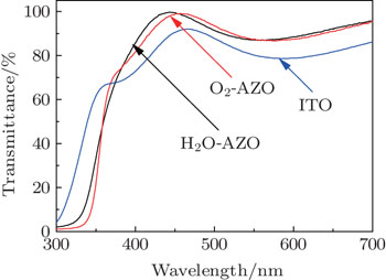
The transmission spectra with a wavelength range from 300 to 700 nm were measured and shown in Fig. 1. Both the AZO-TCLs show a transparency higher than 98% at a wavelength of 450 nm while the ITO-TCL shows 90% transparency. The electrical characteristics of the TCLs on the sapphire substrate are summarized in Table 1, which are measured by van der Pauw Hall effect measurements. Compared with the O2-AZO-TCL with a resistivity of 7 × 10⁻⁴ Ω·cm, the H2O-AZO-TCL shows a lower resistivity of 5 × 10⁻⁴ Ω·cm, which is attributed to the higher mobility (34 cm2·v−1·s−1) and higher carrier concentration (3.6 × 1020 cm−3). In contrast, in spite of the lowest resistivity of ITO, the lower mobility and the higher carrier concentration could result in relatively low transmittance.

Fig. 1. Transmittance spectra of H2O-AZO-, O2-AZO-, and ITO-TCLs on a quartz substrate.
Table 1.

Mobility, carrier concentration, resistivity of various TCLs measured by the van der Pauw Hall effect measurement.

.

In order to understand the origin of the improved conductive properties of the H2O-AZO-TCL, the 2θ to ω x-ray diffraction (XRD) pattern was used to analyze the crystalline structure of both AZO-TCLs grown on the sapphire substrate. As shown in Fig. 2, compared with O2-AZO, the diffraction peak of ZnO (0002) for the H2O-AZO is shifted to a high diffraction angle, indicating that the lattice constant of H2O-AZO is smaller than that of O2-AZO. Here, the diffraction peak intensity was normalized by the maximum value. Considering the smaller radius of Al3+ ions, these results indicate that more Al3+ ions substituted Zn2+ ions into the H2O-AZO lattice, which plays the role of a donor leading to the higher carrier concentration.[12,13] In fact, for H2O-AZO-TCL growth, the molar ratio of TMAl:DEZn is 0.1, which is smaller than that of 0.15 for O2-AZO-TCL growth. The results suggest that when using H2O as an oxidizer, the relatively low growth temperature and reduced reactor pressure decrease the parasitic reaction and probably lead to a more effective incorporation of Al into the AZO. Moreover, it was reported that the carrier transport in AZO-TCL is dominated by grain barrier scattering because of the existence of a high amount of point defects and/or dislocations at grain boundaries.[14] According to the grain barrier limited transport model, the relatively high mobility in H2O-AZO-TCL can be explained. At a high carrier concentration, the grain barrier will become narrow. As a result, the electrons are easy to tunnel, leading to the high mobility. The growth and carrier transport mechanisms of H2O-AZO TCL require further study.
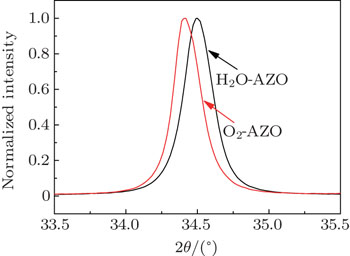
Fig. 2. The 2θ to ω XRD patterns of ZnO (0002) peaks of H2O-AZO- and O2-AZO-TCLs deposited on sapphire substrates.

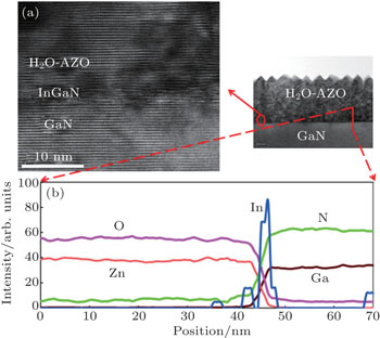
The current–voltage (IV) characteristics of the LEDs with various TCLs were demonstrated. As shown in Fig. 3, the forward voltages (Vf) of LED-I with H2O-AZO-TCL @ 20 mA is as low as 2.82 V, which is a little lower than that of LED-II with O2-AZO-TCL (Vf = 2.87 V @20 mA), and is much lower than that of LED-III with ITO-TCL (Vf = 2.92 V@20 mA). The Vf of LED-I is also much lower than the reported values in literature.[15,16] The linear IV characteristics of the TCL contacts are shown in the inset of Fig. 3. Through CTLM calculation, the specific contact resistances were evaluated to be 2.72 × 10⁻⁴, 2.85 × 10⁻⁴, and 4.6 × 10⁻⁴ for the contacts of the H2O-AZO-TCL, O2-AZO-TCL, and ITO-TCL, respectively. The results indicate that the low Vf is attributed to the good ohmic contact formed between H2O-AZO-TCL and p-GaN with the n+-InGaN contact layer. As reported in our previous work,[6] the epitaxial-like interface was formed between the ZnO-based TCL grown by MOCVD using O2 as an oxidizer and p-GaN with the n+-InGaN contact layer, which contributes to the low specific contact resistance of LEDs. In this work, to confirm the interface properties between H2O-AZO-TCL and p-GaN with the n+-InGaN contact layer, high-resolution transmission electron microscopy (HRTEM) combined with an energy dispersive x-ray (EDX) line scan was also performed. As shown in Fig. 4(a), the epitaxial-like interface with perfect lattice fringes was confirmed between the H2O-AZO-TCL and p-GaN with n+-InGaN. Furthermore, as shown in Fig. 4(b), a 3-nm-thick n+-InGaN tunneling layer was observed by EDX line scan. Namely, the good ohmic contact of H2O-AZO-TCL could also be attributed to the epitaxial-like interface. Considering the similar specific contact resistance and epitaxial-like interface properties of both the AZO-TCLs, the relatively low Vf of LED-I could be mainly attributed to the lower bulk resistivity of H2O-AZO-TCL, which can enhance the lateral current spreading.
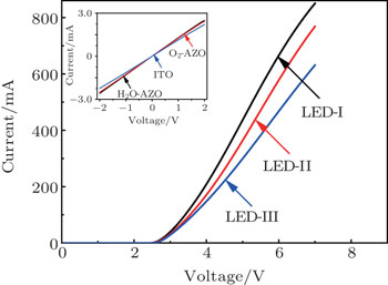
Fig. 3. IV characteristics of LEDs with various TCLs. The inset shows the IV characteristics of H2O-AZO-, O2-AZO-, and ITO-TCLs contacts on p-GaN with n+-InGaN contact layer.
Fig. 4. Cross-sectional HRTEM image (a) and the major element EDX line scan analysis spectra (b) of the H2O-AZO-TCL/n+-InGaN/p-GaN interface.

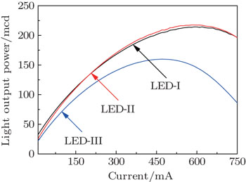
Figure 5 demonstrates the LOP characteristics of the LEDs with various TCLs. As shown in Fig. 5, the light output powers at 20 mA are 39.6, 33.4, and 28.3 mcd for LED-I, LED-II, and LED-III, respectively. At the injection current of 350 mA, the light output powers of LED-I, LED-II, and LED-III were 181.3, 184.6, and 149.9 mcd, respectively. In order to properly evaluate the overall efficiency of the experimental LEDs, the power efficiency of LEDs was defined as the ratio of the optical output power to the electrical input power.[18] As a result, the power efficiency of LED-I with H2O-AZO-TCL was improved by 28.8%@20 mA injection current and 4.92%@350 mA over that of LED-II with O2-AZO-TCL. Moreover, the power efficiency of LED-I was improved by 53.8%@20 mA injection current and 39.6%@350 mA over that of LED-III with ITO-TCL. One can see that the power efficiency of LED-I is markedly higher than that of LED-III. This can be explained by the following reasons: i) the high transmittance of H2O-AZO-TCL over that of ITO-TCL; and ii) the epitaxial-like interface between H2O-AZO-TCL and p-GaN/n+-InGaN with low specific contact resistance. These would enhance the current injection effect and reduce the nonradiative recombination at the interface region. Although the forward voltage of LED-I is slightly lower than that of LED-II, a similar light output power was found. This is presumably attributed to the flat surface of H2O-AZO-TCL. The root mean square roughness of H2O-AZO-TCL is 5.8 nm, which is similar to that of ITO-TCL with the value of 6.3 nm, but is markedly lower than that of O2-AZO-TCL with the value of 11.5 nm. The growth of the H2O-AZO-TCL at relatively low temperatures was presumably dominated by the 2D growth mode.[17] This will result in the smooth surface morphology. Furthermore, LED-III shows the maximum light output power at the injection current of 500 mA and then the light output power declines sharply along with the further increase of the injection current. In comparison, the LEDs with AZO-TCLs (LED-I and LED-II) show the maximum light output power at the injection current of 600 mA, and then the output power declines slowly along with the further increase of the injection current. This can be attributed to the better current spreading in AZO-TCLs with the low contact resistance. These results indicate that the AZO-TCLs grown by MOCVD are more suitable for high-power LEDs.

Fig. 5. Light output power of the LEDs with various TCLs as a function of injection current.
4. Conclusions

In conclusion, an AZO-TCL with high conductivity and high transparence was grown by MOCVD using H2O as an oxidizer at temperatures as low as 400 °C. It was used as TCLs in InGaN/GaN MQW LEDs. Compared with LEDs with O2-AZO-TCL and ITO-TCL, the LEDs with H2O-AZO-TCL exhibit a low Vf and a high power efficiency. In addition to the epitaxial-like interface between the H2O-AZO-TCL and the p-GaN with n+-InGaN contact tunneling layer, these results could be attributed to the lower bulk resistivity of H2O-AZO-TCL. Considering the low cost of H2O-AZO-TCL, the AZO-TCL grown by MOCVD using H2O as an oxidizer will make a great contribution to the production of low-cost and high-efficiency GaN-based LEDs.

Reference
1Zhao YFan B FChen Y TZhuo YPang Z JLiu ZWang G 2016 Chin. Phys. 25 078052
2Liu M GWang Y QYang Y BLin X QXiang PChen W JHan X BZang W JLiao QLin J LWu Z SLiu YZhang B J 2015 Chin. Phys. 24 038503
3Oh B YJeong M CLee WMyoung J M 2005 J. Cryst. Growth 274 453
4Tun C JSheu J KPong B JLee M LLee M YHsieh C KHu C CChi G C 2006 IEEE Photon. Technol. Lett. 18 274
5Yan J TChen C HYen S FLeeC T 2010 IEEE Photon. Technol. Lett. 22 146
6Yang J CPei Y LFan B FHuang S JChen Z MTong C SLuo H TLiang JWang G 2015 IEEE Electron Dev. Lett. 36 372
7Triboulet RPerrie’re J 2003 Progress in Crystal Growth and Characterization of Materials 47 65
8Pan MFenwick W EStrassburg MLia NKang HKane M HAsghar A 2006 Journal of Crystal Growth 287 688
9Bugnon GNicolay SDing LDespeisse MHedler AEberhardt JWachtendorf CBallif C 2011 Solar Energy Materials & Solar Cells 95 2161
10Ding LBoccard MBugnon GBenkhaira MNicolay SDespeisse MMeillaud FBallif C 2012 Solar Energy Materials & Solar Cells 98 331
11Nicolay SBenkhaira MDing LEscarre JBugnon GMeillaud FBallif C 2012 Solar Energy Materials & Solar Cells 105 46
12Park K CMa D YKim K H 1997 Thin Solid Films 305 201
13Oh B YJeong M CLee WMyoung J M 2005 J. Cryst. Growth 274 453
14Ellmer KMientus R 2008 Thin Solid Films 516 5829
15Park T YChoi Y SKang J WJeong J HPark S JJeon D MKim J WKim Y C 2010 Appl. Phys. Lett. 96 051124
16Yen K YChiu C HLi C WChou C HLin P SChen T PLin T YGong J R 2012 IEEE Photon. Technol. Lett. 24 2105
17Zhang B PWakatsuk KBinh N TUsam NSegawa Y 2004 Thin Solid Films 449 12
18Sheu J KLee M LLu Y SShu K W 2008 IEEE J. Quantum Electron. 44 1211